Flash memory
TI-84 Plus OS 2.55MP — Flash hardware, boot bcalls, and archive writes.
The TI-84 Plus programs Flash through three distinct layers: ASIC access control, an AMD-compatible command state machine in the Flash chip, and boot-page bcalls that execute their write loops from RAM. This page separates those layers, gives calling conventions and examples for the Flash bcalls, reconstructs their workers byte for byte, and follows a normal Archive prgmA operation into the hardware path.
Evidence layers
The mechanisms below use several evidence sources. A claim marked [confirmed] comes from the local OS 2.55MP image or a complete TilEm execution trace. A claim marked [standard] comes from the named hardware source and agrees with the ROM. Emulator behavior is identified explicitly. It establishes what that emulator implements, not what the physical ASIC or Flash chip does.
| Layer | Main evidence | What it establishes |
|---|---|---|
| TI-OS and boot code | tools/rom.bin, especially 3D:61AF–3D:6BC4 and 3F:4784–3F:4E56 | bcall ABI, guards, RAM workers, archive allocation, and status handling [confirmed] |
| Dynamic execution | archive and GCFLASH TilEm traces plus guarded TilEm, Wabbitemu, and MAME runs | ROM worker paths, GC sector ordering, execution limits, and native command-state behavior [confirmed] for the pinned emulator runs |
| ASIC model | TilEm x4_memory.c, x4_io.c, and x4_init.c | protected-byte recognizer, port gates, execution limits, and modeled sector protection [standard] |
| Flash device | Datamath’s March 2004 board photograph and Fujitsu MBM29LV800TA data sheet | observed package marking, sector geometry, command cycles, DQ status semantics, and rated limits [standard] |
| Emulator comparison | pinned TilEm, Wabbitemu, MAME, and jsTIfied source | modeled command decode, mutation rules, status reads, timing, and missing ASIC gates [standard] |
Write-layer schematic. Bcall entry guards, remaining caller obligations, and RAM-worker execution are [confirmed]. ASIC gate details and the AMD-compatible command state machine are [standard].
Physical organization
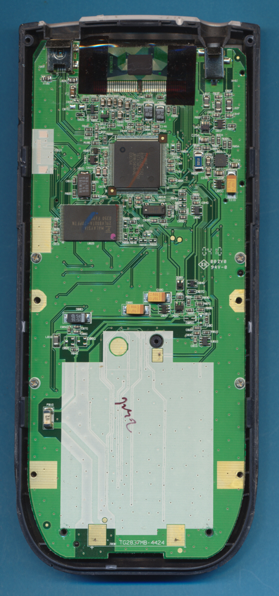
Identified board part and compatible family
Datamath’s photographed March 2004 TI-84 Plus board carries a Fujitsu package
marked 29LV800TA-70PFTN. Fujitsu’s orderable part number adds its MBM
prefix: MBM29LV800TA-70PFTN. This identifies the device on that photographed
board. It does not establish one vendor for every TI-84 Plus revision.
[standard]
Datamath’s NOR component index also lists AMIC A29L800A, Fujitsu 29LV800,
Spansion S29AL008D, and Macronix MX29LV800 as compatible 1 MiB families.
Those entries establish a reported compatible family, not which part a
particular calculator contains. [standard]
The Fujitsu suffixes and rated limits decode as follows. These are data-sheet limits rather than measurements of a calculator. [standard]
| Marking or field | Meaning |
|---|---|
8M (1M × 8/512K × 16) | 8 Mbit array, used here as one MiB of byte-addressable NOR Flash |
TA | top-boot sector geometry |
-70 | 70 ns maximum read access |
PFTN | 48-pin TSOP(I), normal-bend package |
| supply | 3.0 V-only read, program, and erase |
| program/erase endurance | minimum 100,000 cycles |
| byte program | 8 µs typical, 300 µs maximum |
| sector erase | 1 s typical, 10 s maximum |
The local ROM image and TilEm’s TI-84 Plus model use 64 logical pages of
16 KiB. A logical Flash page is an ASIC paging unit, not an erase unit. Port
0x06 maps one page into the Z80’s 0x4000–0x7FFF bank-A window. The Flash
device erases the larger physical sector containing the command address.
[confirmed] for the ROM page count; [standard] for the device organization.
Data-sheet command and status interface
In byte mode, the Fujitsu device decodes unlock addresses 0xAAA and 0x555.
The command table defines the following operations. Address and data cycles
after a command prefix are shown separately. [standard]
| Operation | Byte-mode command cycles |
|---|---|
| Read/reset | F0, or AA 55 F0 |
| Autoselect | AA 55 90 |
| Byte program | AA 55 A0, then destination and data |
| Chip erase | AA 55 80 AA 55 10 |
| Sector erase | AA 55 80 AA 55 30 |
| Erase suspend | B0 at any address during sector erase or its timeout window |
| Erase resume | 30 at any address while erase is suspended |
| Enter fast mode | AA 55 20 |
| Fast program | A0, then destination and data; repeat in fast mode |
| Exit fast mode | 90, then F0 or 00 |
The data sheet defines no CFI query command for this part. A reset returns the device to array-read mode, including after DQ5 reports an exceeded timing limit. [standard]
The status outputs distinguish more states than the boot workers consume: [standard]
| Bit | Fujitsu data-sheet behavior |
|---|---|
| DQ7 | complements programmed data bit 7 while program is active; reads 0 during erase and the array value after completion |
| DQ6 | toggles during program, erase, and the sector-erase timeout window |
| DQ5 | indicates exceeded program/erase timing; it can also follow an attempt to program a nonblank location without erasing |
| DQ3 | distinguishes the open sector-erase command window from the active erase algorithm |
| DQ2 | toggles for an erasing or erase-suspended sector and helps distinguish erase states from program states |
Erase suspend applies only to sector erase, including its 50 µs timeout window. The device ignores it during chip erase and byte program. The data sheet bounds suspend latency at 20 µs. DQ7 becomes one and DQ6 stops toggling; DQ2 continues toggling when the suspended sector is read. Reads and programs remain available in sectors that are not being erased. [standard]
Fujitsu autoselect returns manufacturer 0x04 and top-boot byte-mode device
0xDA at byte-mode offsets XX00 and XX02. Offset XX04 reports the
selected sector’s protection state in DQ0. Wabbitemu and MAME instead return
manufacturer 0x01 with the same device code. Their values identify an
AMD-compatible emulator model, not the Fujitsu package in the Datamath
photograph. [standard]
Retail ROM command coverage
The retail ROM’s instruction-aligned direct stores to logical unlock addresses
0x6AAA and 0x5555 occur at 11 locations. They belong to three
length-prefixed command bodies. [confirmed]
| Command body | Direct unlock-address stores | Command use |
|---|---|---|
Page-3D program worker at 3D:730A | 3D:7342, 3D:734B, 3D:7354 | AA 55 A0, then program data through LDI |
| Boot erase worker | 3F:4C48, 3F:4C51, 3F:4C5A, 3F:4C63, 3F:4C6C | AA 55 80 AA 55 30 |
| Boot program worker | 3F:4CFB, 3F:4D04, 3F:4D0D | AA 55 A0, then program data through LDI |
No direct unlock-address candidate has a nearby command-valued LD A,n for
chip erase (0x10), fast-mode entry (0x20), autoselect (0x90), erase
suspend (0xB0), or CFI query (0x98). The worker bodies use byte program,
sector erase, and array reset. [confirmed]
tools/ti84re/flash/rom_commands.py performs the structural match, and
tools/ti84re/flash/analyze_rom_commands.py emits text or JSON. The scan deliberately
does not treat raw literals as commands. Linear disassembly can decode data as
instructions, indirect stores can hide a destination, and a standalone command
can target an address other than the two unlock addresses. The result therefore
establishes coverage of exact LD (nn),A candidates, not universal absence of
every dynamically constructed command. [confirmed]
Sector geometry
The Fujitsu MBM29LV800TA data sheet defines the top-boot geometry below.
TilEm, Wabbitemu, MAME, and jsTIfied use the same boundaries. [standard]
| Physical range | Size | Logical pages or page portion |
|---|---|---|
0x000000–0x0EFFFF | 15 × 64 KiB | pages 00–3B, four pages per sector |
0x0F0000–0x0F7FFF | 32 KiB | pages 3C–3D |
0x0F8000–0x0F9FFF | 8 KiB | 3E:4000–3E:5FFF |
0x0FA000–0x0FBFFF | 8 KiB | 3E:6000–3E:7FFF |
0x0FC000–0x0FFFFF | 16 KiB | page 3F |
The two halves of logical page 3E are separate 8 KiB sectors. This is why _EraseCertificateSector accepts logical address 0x4000 or 0x6000. Page 3F is one 16 KiB boot sector. A sector erase directed anywhere in an ordinary archive page erases all four 16 KiB pages in its 64 KiB sector. [confirmed] for the certificate API; [standard] for chip geometry.
Three independent protection mechanisms
“Flash protection” can refer to three different controls. Treating them as one switch obscures several ROM checks.
Flash command lock — port 0x14
Port 0x14 controls whether writes reach the Flash command state machine. Writing 1 unlocks Flash command writes; writing 0 locks them. The write is accepted only after the ASIC observes this byte sequence fetched from a privileged Flash region: [standard]
00 00 ED 56 F3 D3
The usual instruction spelling is:
nop
nop
im 1
di
out (0x14),a
The ASIC recognizes fetched bytes rather than the semantic instruction stream. WikiTI documents alternate instruction sequences that produce the same bytes. TilEm’s TI-84 Plus model advances its recognizer only when the bytes come from physical 0xB0000–0xBFFFF or 0xF0000–0xFFFFF; other Flash or RAM reads reset the recognizer. It accepts the following port-0x14 output only in recognizer state 7. [standard]
Unlocking port 0x14 does not program a byte. It allows subsequent memory writes to reach the Flash chip, where they must still form a valid AMD command sequence. [standard]
The public write and erase bcalls expect Flash to be unlocked by their caller. The archive record writer at 3D:64AA performs the protected port-0x14 sequence itself before calling those APIs. [confirmed]
Physical sector protection
TilEm assigns protection group 1 to physical 0xB0000–0xBFFFF and 0xFC000–0xFFFFF. Port 0x21 bits 0–1 select the modeled override group while Flash is unlocked. A command can therefore pass the port-0x14 lock and still be rejected for a protected physical sector. [standard]
The retail boot programs port 0x21 = 0 at 3F:41DC. Its low field also
selects model-specific Flash page bounds, while bits 4–5 configure the RAM
execution mask. See ASIC status, identity, protection, and GPIO
for the ROM uses, emulator equations, and public size tables. [confirmed] for
the boot write; [standard] for the modeled protection behavior.
This protection is separate from the safe bcall checks. For example, _WriteAByte permits starting page 3E at the software layer, while the hardware still controls whether the affected sector is writable. [confirmed] for the bcall; [standard] for the ASIC model.
Read and execution protection
The certificate page is read-censored while Flash is locked. WikiTI documents the model-selected page as 1E, 3E, or 7E; TilEm returns 0xFF for locked reads of page 3E on its TI-84 Plus model. [standard]
Ports 0x22 and 0x23 define a forbidden Flash-execution interval. TilEm
includes both endpoints, while Wabbitemu allows the lower page. The retail boot
writes 0x08 and 0x29. Ports 0x25 and 0x26 bound executable RAM in 1 KiB
units. Both emulators accept writes to these protected ports only while Flash
is unlocked. See Execution protection for the ROM
sequence, exact equations, guarded Flash and RAM execution runs, and unresolved
physical boundaries. [confirmed] for the boot values and pinned emulator runs;
[standard] for the source models.
These execution limits explain why the byte-poke loops run at ramCode (0x8100). They are distinct from the Flash chip’s inability to provide ordinary array data while a program or erase operation is active. [confirmed] for the RAM workers; [standard] for the execution controls.
Boot-page Flash API
The retail boot bcall table maps the Flash APIs below. The bcall ID is the word after rst 28h; the body address is where the resolved code executes. [confirmed]
| Bcall | ID | Body | Inputs | Intended distinction |
|---|---|---|---|---|
_WriteAByte | 8021 | 3F:4C9F | A page, DE destination, B byte | one byte; permits page 3E, rejects page 3F |
_EraseFlash | 8024 | 3F:4C2A | A page, HL address in the sector | raw sector selector; no page guard |
_EraseCertificateSector | 8060 | 3F:4E3F | H=0x40 or H=0x60; L unchecked | select one 8 KiB certificate sector; hides erase result |
_EraseFlashPage | 8084 | 3F:4C1E | A page | use 0x4000 in that page; rejects page 3E |
_WriteFlashUnsafe | 8087 | 3F:4CA6 | A page, DE destination, BC length, HL RAM source | block write; permits page 3E, rejects page 3F |
_WriteAByteSafe | 80C6 | 3F:4C9A | A page, DE destination, B byte | one byte; rejects pages 3E and 3F |
_WriteFlash | 80C9 | 3F:4C8F | A page, DE destination, BC length, HL RAM source | block write; rejects pages 3E and 3F |
_SetFlashLowerBound | 80CF | 3F:4784 | A value for port 0x23 | change an execution-protection bound; leaves interrupts disabled |
WikiTI’s ABI agrees with these register uses and says the block-write source must be RAM. The ROM adds exact page guards, call-site checks, return values, and boundary behavior described below. [standard] for the published ABI; [confirmed] for the additions.
Programmer-facing bcall guide
The bcall-level guide — entry contracts, register conventions, worker
selection, and executable examples for _WriteFlash, _WriteAByte,
_EraseFlash, and their neighbors — is on Flash bcall programming
guide.
_WriteFlash entry paths
The four write entry points converge on the core at 3F:4CA6. [confirmed]
flowchart TD
    WF["_WriteFlash · 3F:4C8F<br/>mask page; reject 3E"] --> U["_WriteFlashUnsafe · 3F:4CA6"]
    WS["_WriteAByteSafe · 3F:4C9A<br/>mask page; reject 3E"] --> W1["_WriteAByte · 3F:4C9F<br/>copy B to OP1; BC=1"]
    W1 --> U
    U --> G["direct-call and page-3F guards"]
    G --> R["copy worker to 0x8100 and execute"]
Safe and unsafe page guards
_WriteFlash masks A with 0x3F and returns immediately for page 3E. _WriteAByteSafe does the same before falling into _WriteAByte. The unsafe core masks the page again and returns for page 3F. Safe writes therefore reject both pages 3E and 3F. [confirmed]
_WriteAByte enters the unsafe core without the page-3E test. It stores B in OP1 at 0x8478, replaces HL with that address, and sets BC=1. It permits page 3E but still inherits the page-3F rejection. [confirmed]
The page guards return the result of an equality comparison. Rejected page
3E and page 3F calls therefore return Z, the same condition as a successful
worker. Callers must obey the page contract; Z alone does not prove that a
write occurred. [confirmed]
Direct-call-site check
Both _WriteFlashUnsafe and _EraseFlash inspect the immediate stacked return address:
ex (sp),hl
bit 7,h
ex (sp),hl
ret nz
The routine returns NZ when that address is at least 0x8000. It does so
before masking A. A normal bcall passes because the bcall dispatcher
interposes a low-memory return frame; the archive trace reaches 3F:4CA6 with
the relevant return address at 0x2B41. This is a direct-call-site check. It
does not prevent a RAM program from invoking the public bcall through
rst 28h. [confirmed]
Zero-length write
After the guards, _WriteFlashUnsafe saves AF, tests B|C, and restores
AF when the length is zero. A zero-length call therefore returns the masked
page in A and the flags from the preceding CP 0x3F. An accepted page is not
equal to 0x3F, so this no-op returns NZ. It never copies or executes the RAM
worker. [confirmed]
Early-return trace
The read-only entry-returns fixture runs on the unmodified ROM. It verifies
the first eight bytes at 3F:4CA6, never writes port 0x14, and exercises
four paths that return before worker launch. ti84re.flash.analyze_trace reports
zero CPU write attempts targeting mapped Flash. The captured bcall-visible
values are: [confirmed] for
TilEm execution of the ROM paths.
| Clock | Call and trigger | Return AF | Condition |
|---|---|---|---|
| 186,993,567 | _WriteFlash, input page 0x7E → masked page 3E | 0x3E42 | Z |
| 186,995,033 | _WriteFlashUnsafe, input page 0x7F → masked page 3F | 0x3F42 | Z |
| 186,996,552 | _WriteFlashUnsafe, input page 0x7D, BC=0 | 0x3DBB | NZ |
| 186,996,732 | direct CALL 3F:4CA6 from RAM, input A=0xA5 | 0xA591 | NZ |
The direct call reaches 3F:4CA6 and returns from 3F:4CAA; it does not reach
the page mask at 3F:4CAB. The zero-length call reaches 3F:4CB3, branches to
3F:4CC6, restores the saved comparison result, and returns. [confirmed]
Byte-entry return trace
_WriteAByteSafe checks page 3E before entering _WriteAByte. A page-3E
rejection returns from 3F:4C9E without changing OP1, BC, DE, or HL.
Page 3F passes that first comparison. _WriteAByte then stores B at
OP1 (0x8478), loads HL=0x8478 and BC=1, and reaches the unsafe core.
The page-3F rejection at 3F:4CAF therefore exposes those wrapper side
effects even though no worker runs. [confirmed]
A direct CALL 3F:4C9F from RAM also performs the byte-wrapper setup before
the unsafe core inspects the return address at 3F:4CA6. It returns from
3F:4CAA with OP1, BC, and HL changed. [confirmed]
The read-only byte-entry-returns fixture verifies all 16 bytes from
3F:4C9A through 3F:4CA9 on the unmodified ROM. It restores the original
OP1 byte before returning and never unlocks Flash. Its machine-code SHA-256
is 6851da991e031ea7df1a31ab3bf62816ad992e3d1946566d31b0a02e16dd50e1.
The trace contains zero CPU write attempts targeting mapped Flash. [confirmed]
for the fixture and TilEm execution.
| Clock | Call and trigger | Return AF | BC | DE | HL | OP1 |
|---|---|---|---|---|---|---|
| 187,804,393 | _WriteAByteSafe, page 0x7E → 3E | 0x3E42 | 0x2233 | 0x4455 | 0x6677 | 0x11 unchanged |
| 187,806,001 | _WriteAByteSafe, page 0x7F → 3F | 0x3F42 | 0x0001 | 0x6677 | 0x8478 | 0x44 from B |
| 187,807,587 | _WriteAByte, page 0x7F → 3F | 0x3F42 | 0x0001 | 0x7788 | 0x8478 | 0x55 from B |
| 187,807,892 | direct CALL 3F:4C9F, A=0xA5 | 0xA591 | 0x0001 | 0x8899 | 0x8478 | 0x66 from B |
The two page guards still return Z. That condition describes the final
comparison, not whether _WriteAByte changed its scratch registers or launched
a worker. [confirmed]
RAM-worker launcher
boot_ram_worker_launcher at 3F:48C5 launches length-prefixed boot workers.
IX points at this packed descriptor: [confirmed]
typedef struct {
    uint16_t length;
    uint8_t code[];
} RamWorkerDescriptor;
The flexible code[] member describes the serialized ROM object. Ghidra applies
the reusable type to the two-byte header only because each payload has a
different length; the payload begins at descriptor + 2. The launcher copies
descriptor->length bytes from there to ramCode at 0x8100. It then restores
the caller’s HL, DE, and BC and calls the copied code. [confirmed]
The interrupt wrapper at 3F:48EE records IFF2 from LD A,I in 0x82A2, disables interrupts, and returns to the launcher. After the worker returns, 3F:48E1 executes EI only if interrupts were enabled before entry. The worker therefore runs atomically while preserving the caller’s prior interrupt-enabled state. [confirmed]
| Worker | Prefix | Source bytes | RAM destination |
|---|---|---|---|
| sector erase | boot_flash_erase_worker_descriptor at 3F:4C3B, 0x0052 | descriptor + 2, at 3F:4C3D–3F:4C8E | ramCode–ramCode + 0x51 |
| block program | flash_program_worker_descriptor at 3F:4CC8, 0x007C | flash_program_worker_code at 3F:4CCA–3F:4D45 | ramCode–ramCode + 0x7B |
Page 3D contains a relocated copy of the launcher at 3D:678C. It runs
flash_to_ram_worker_descriptor at 3D:6761 and
certificate_worker_descriptor at 3D:7308. Its interrupt wrapper at
3D:67B5 has the same IFF2-save, DI, conditional-EI behavior as the boot
launcher. The inferred name ram_worker_launcher therefore describes both
call paths. [confirmed]
Block-program worker
The block worker repeats a four-write AMD byte-program sequence for each source byte. It temporarily maps fixed pages 02 and 01 so the command addresses appear in bank A, then restores the target page for the data write. [confirmed]
| Step | Mapped page | Logical write | Value |
|---|---|---|---|
| 1 | 02 | 0x6AAA | 0xAA |
| 2 | 01 | 0x5555 | 0x55 |
| 3 | 02 | 0x6AAA | 0xA0 |
| 4 | target | DE | byte from (HL) |
The device decodes the physical low 12 address bits. Page 02, logical
0x6AAA is physical address 0xAAAA; page 01, logical 0x5555 is physical
0x5555. Their low 12 bits are the Fujitsu byte-mode unlock addresses 0xAAA
and 0x555. [confirmed] for the ROM addresses; [standard] for device decoding.
Completion polling
After LDI writes a byte and advances HL, DE, and BC, the worker steps back to compare the programmed byte with the target read: [confirmed]
- XOR source and target, then test bit 7. Equal DQ7 means the byte completed.
- If DQ7 differs, restore that same target byte and test its DQ5 bit.
- Clear DQ5 repeats the first target read.
- Set DQ5 causes one final target read and DQ7 comparison.
- A second DQ7 mismatch takes the failure path.
This is the algorithm in Fujitsu figure 22. During programming, DQ7 returns the complement of the requested data bit until completion. DQ5 indicates an exceeded timing limit. The data sheet requires the second DQ7 check because DQ7 and DQ5 may change simultaneously. [standard]
Return state
On success, the worker writes reset command 0xF0 at the last target address,
forces port 0x06 to page 3F, and returns A=0, Z. On failure,
3F:4D3D–3F:4D45 writes 0xF0 at the failing target, loads A=0x3F for
the page-select output, executes OR A, and returns A=0x3F, NZ. [confirmed]
After full success, HL and DE point one byte beyond the completed span, and
BC=0. On failure, the branch occurs before 3F:4D2C and 3F:4D2D restore
the backed-up pointers. HL and DE therefore identify the failing source and
target bytes, while BC retains the decrement performed by LDI.
_WriteAByte destroys all three public ABI registers. [confirmed]
Forcing page 3F is part of the worker ABI. The outer bcall dispatcher restores the page mapping required by its caller after the boot routine returns. A direct caller that passes the low-address check must account for this mapping change itself. [confirmed]
Internal certificate-page programmer
certificate_write_byte at 3D:72E5 launches a second byte-program worker.
It sets BC=1, clears (IY+0x25).1, normalizes the target page for the current
calculator model, and passes certificate_worker_descriptor to
ram_worker_launcher. Its code begins at descriptor + 2 and contains 129
bytes at 3D:730A–3D:738A. flash_program_worker_code contains 124 bytes at
3F:4CCA–3F:4D45. [confirmed]
The only direct call to certificate_write_byte is 3D:4332, inside
certificate_copy_from_flash at 3D:431A. The loop obtains an ordinary Flash
page from 3D:5258, stages one byte in OP1 with _FlashToRam, selects the
model-specific certificate page through model_certificate_page at 3D:738B,
and programs the byte at the current certificate destination. Direct callers
at 3D:426A and 3D:4715 reach this loop. [confirmed]
certificate_copy_to_flash at 3D:434B performs the reverse transfer. Its
prologue at 3D:433F obtains and erases the ordinary Flash destination page.
The loop stages a certificate byte in OP1 through 3D:42AC, obtains the
ordinary destination page through 3D:5258, and calls _WriteFlashUnsafe = 8087h. The direct callers at 3D:4127 and 3D:4707 pass destination address
0x4000. [confirmed]
Both loops belong to certificate_rebuild_dispatch at 3D:40F1. The
dispatcher stores its mode byte at 0x9C20, copies certificate data to an
ordinary Flash work area at 3D:4127, rebuilds mode-dependent certificate
fields, erases a model-selected certificate half through 3D:4252, and can
copy the work area back at 3D:426A. This identifies the data directions and
the rebuild role. Direct calls and page-0 bjump calls identify an owner for
each mode. [confirmed]
The dispatcher operates on the last 0x216 bytes of either 8 KiB certificate
half. Its fixed offsets and lengths divide that tail into four contiguous
blocks: [confirmed]
| Half-relative offset | Length | Range |
|---|---|---|
0x1DEA | 0x66 | 0x1DEA–0x1E4F |
0x1E50 | 0xC8 | 0x1E50–0x1F17 |
0x1F18 | 0xC8 | 0x1F18–0x1FDF |
0x1FE0 | 0x20 | 0x1FE0–0x1FFF |
The adjacent App-restriction bytes make the complete decoded tail easier to
address as a partial structure based at half offset 0x1DD2: [confirmed]
typedef struct {
    uint8_t restriction_control;        // +0x000, half offset 0x1DD2
    uint8_t restriction_record[13];     // +0x001, half offset 0x1DD3
    uint8_t unresolved_1de0_1de9[10];   // +0x00E
    uint8_t gc_recovery[0x66];          // +0x018, half offset 0x1DEA
    uint8_t ti84_app_trials[0xC8];      // +0x07E, half offset 0x1E50
    uint8_t alternate_model_span[0xC8]; // +0x146, half offset 0x1F18
    uint8_t validity[0x20];             // +0x20E, half offset 0x1FE0
} CertificateMetadataTail;
The unresolved_1de0_1de9 name deliberately records only its bounds. The ROM
evidence does not identify an owner for those ten bytes. The notation below
uses certificate_tail for a CertificateMetadataTail view of the selected
certificate half. BuildTypes.java registers this reusable type but does not
apply it at one fixed address: the ROM selects the certificate half at runtime,
so certificate_tail means a conceptual pointer to selected_half + 0x1DD2,
not a global Ghidra symbol. [confirmed]
Six helpers at 3D:5227–3D:5256 add fixed or model-selected offsets to
_GetCertificateStart’s result. Raw CALL scanning finds the complete direct
caller sets without relying on disassembler labels: [confirmed]
| Entry | Selected offset | Direct callers |
|---|---|---|
3D:5227 | 0x1DD3 | 3D:42D4, 3D:7D7A |
3D:522D | 0x1FE0 | 3D:42B3, 3D:4589, 3D:4654, 3D:47A8, 3D:521D, 3D:5448 |
3D:5233 | 0x1F18 | 3D:414B, 3D:4288, 3D:42EA, 3D:42F2, 3D:42FD, 3D:4306, 3D:47B1, 3D:493D, 3D:4CBD, 3D:4F14, 3D:5080, 3D:5184, 3D:51A8, 3D:538F |
3D:5241 | 0x1DEA | 3D:4274, 3D:4298, 3D:42A3 |
3D:5247 | model-selected | 3D:490F, 3D:5385, 3D:548F, 3D:5C0E |
3D:5252 | 0x1FE0 | 3D:430E |
The model-selected helper calls 00:1837. That probe reads port 0x02, masks
bit 7, then executes XOR 0x80. It returns Z when bit 7 was set and NZ
when it was clear, while restoring A and BC.
3D:5247 branches to the fixed 0x1F18 helper when the bit is clear and falls
through to 0x1E50 when it is set. The resolved TI-84 Plus traces read 0xE1,
0xE3, or 0xE7, so every observed TI-84 Plus state selects 0x1E50.
[confirmed]
Wabbitemu independently returns a base value with bit 7 set for models at or
above its TI_84P enum and clear for its TI-83 Plus family. This supports the
family split implemented by the ROM but remains evidence about the emulator,
not a physical measurement. [standard]
Consequently certificate_tail.ti84_app_trials, at
0x1E50–0x1F17, is the active App-trial table on TI-84 Plus.
When port-0x02 bit 7 is clear, the same clear, write, query, and display paths
select certificate_tail.alternate_model_span at
0x1F18–0x1FDF. TI-84 Plus rebuild modes 0
and 2 still stage or replace that alternate-model span together with validity
metadata, but no TI-84 Plus per-entry semantic accessor to that span has been
identified. Giving it another TI-84 Plus field name would exceed the evidence.
[confirmed] for selection and access; [hypothesis] for any further TI-84 Plus
meaning.
The helper calls in each dispatch branch identify which span receives
mode-specific replacement data. Other helpers clone retained spans from the
active half to the opposite half. Mode 4 also exports 0x1E50–0x1F17 to
0x8000 and 0x1DD3–0x1DDF to 0x80F0. [confirmed]
| Mode | Branch | Mode-specific replacement span |
|---|---|---|
0 | 3D:423F | 0x1F18–0x1FFF (0xE8 bytes) |
1 | 3D:41ED | 0x1E50–0x1F17 (0xC8 bytes) |
2 | 3D:41DF | 0x1F18–0x1FFF (0xE8 bytes) |
3 | 3D:41FB | 0x1DEA–0x1E4F (0x66 bytes) |
4 | 3D:4209 | 0x1DEA–0x1E4F and 0x1FE0–0x1FFF |
5 | 3D:421D | 0x1FE0–0x1FFF (0x20 bytes) |
6 | 3D:422B | complete 0x1DEA–0x1FFF tail (0x216 bytes) |
Neither copy loop nor the dispatcher writes port 0x14. Five direct call
sites enter the dispatcher: [confirmed]
| Mode | Direct call | Byte-pinned gate context |
|---|---|---|
0 | 3D:66C7 | The full-reset path at 35:7205 reaches 3D:6673 through the page-0 trampoline at 00:2DC3. 3D:6673 opens the gate at 3D:6680; the tail at 3D:66CA jumps to the shared relock routine. |
1 | 3D:5774 | The App-deletion path at 3D:4018 and invalid-App cleanup at 3D:5F71 call 3D:5759. The first path opens at 3D:400A; the second opens at 3D:5F28. |
2 | 3D:437E | The certificate receive path reaches 3D:4721; Flash App receive preparation reaches 3D:5094. Both inherit gate state. |
5 | 3D:51D7 | The enclosing path opens at 3D:70DA; later exits relock at 3D:7194, 3D:71AA, or 3D:71E4. |
6 | 3D:7D87 | _RemoveAppRestrictions at 3D:7C1B opens at 3D:7C46, calls the rebuild wrapper at 3D:7D82, and relocks at 3D:7C8C. |
Modes 3 and 4 enter through the page-0 bjump stub at 00:2B77. The stub’s
inline descriptor is F1 40 7D, which resolves to 3D:40F1. Both callers
belong to gc_recovery_preflight at 3C:7219, which opens the Flash gate at
3C:7228: [confirmed]
| Mode | Page-3C call | Call chain | Role |
|---|---|---|---|
3 | 3C:7558 | 3C:7219 → 3C:724A → 3C:7544 → 3C:7558 → 00:2B77 → 3D:40F1 | Rewrite the 0x1DEA–0x1E4F recovery metadata after an archive-sector operation in the recovery loop. |
4 | 3C:7313 | 3C:7219 → 3C:72A5 → 3C:7313 → 00:2B77 → 3D:40F1 | Initialize the certificate-backed recovery metadata before the loop. |
Mode 0 initializes the OS/App-validity tail during full reset. 3D:6673
erases ordinary Flash page 8, fills the 0xE8-byte replacement buffer with
0xFF, and stores 0xFE at 0x836D. That RAM byte corresponds to
certificate offset 0x1FE0. On models other than the TI-83 Plus, the routine
also stores 0x7F in the next byte before invoking mode 0. [confirmed]
Mode 1 clears a two-byte per-App trial entry when an App is removed. 3D:5759
stages the model-selected table, converts the App page to a two-byte index,
writes FF FF, and invokes mode 1. On TI-84 Plus that table is
0x1E50–0x1F17. The table’s use as an App trial table is also ROM-confirmed.
The App receive path writes the same
two-byte entry at 3D:5BB7. The App-information path at 36:70B5 calls the
reader at 3D:5466, displays the ROM string "Trials Remaining:" at
01:41AA, and prints values derived from the two bytes. The direct mode-1
callers at 3D:4018 and 3D:5F71 belong to App deletion and invalid-App
cleanup. [confirmed]
One mode-2 owner is the certificate receive path. The link header dispatcher
selects certificate type 0x25 at 3C:565D. After _FindFirstCertField, a
field selector with H=3 and L & 0xF0 = 0x10 reaches the page-0 bjump stub
at 00:2BFB from 3C:5714. That stub targets 3D:4771. Its certificate-half
rotation path calls 3D:46EE, which invokes mode 2 at 3D:4721. This pins
mode 2 to rebuilding 0x1F18–0x1FFF for that certificate-field selector.
The other mode-2 caller belongs to Flash App receive preparation. Header
type 0x24 enters at 3C:550D. The per-page call at 3C:55BD reaches
3D:73BE through the page-0 stub at 00:2D81. 3D:73BE checks the App page,
clears its App-validity bit when necessary, and reaches 3D:5019 through
3D:5356. That path stages 0x1F18–0x1FFF and invokes mode 2 at
3D:5094. [confirmed]
These owners establish where mode 2 is used. They do not establish any
additional TI-84 Plus field meaning for the alternate-model App-trial span at
0x1F18–0x1FDF. [hypothesis] for such an additional meaning.
The mode-4 path fills the model-selected journal buffer at 0x82A5 or
0x8000, initializes its phase bytes at 3C:72D1–3C:730D, and invokes the
dispatcher. The recovery loop reaches mode 3 through 3C:7544. That routine
selects an archive sector, calls _EraseFlashPage = 8084h, updates the RAM
journal fields at 3C:7568 and 3C:7576, then persists the 0x66-byte block.
[confirmed]
The main bcall table pins mode 6 to the App-restriction API: [confirmed]
| Bcall | ID | Page-3D entry |
|---|---|---|
_SetAppRestrictions | 52F6h | 3D:7B9B |
_RemoveAppRestrictions | 52F9h | 3D:7C1B |
_QueryAppRestrictions | 52FCh | 3D:7CBA |
certificate_tail.restriction_control occupies certificate offset
0x1DD2. The 13-byte restriction_record field at 0x1DD3–0x1DDF acts as
a record or as an App-restriction bitmap, depending on the API operation. For an
App on Flash page $p$, the bitmap index is $p - 8$. 3D:7D69 divides that
index by eight, and the mask helper at 3D:785D uses least-significant-bit-first
ordering. A clear bitmap bit means that the App is restricted. [confirmed]
The low control-byte bits have these ROM-confirmed roles:
| Bit | Mask | Clear-bit meaning | Evidence |
|---|---|---|---|
0 | 0x01 | Base restriction control is active. | The type-2 set and query paths at 3D:7C02 and 3D:7CD8; aggregate type 3 is queried by _ExecutePrgm at 07:5758, while equation/token paths query type 2. |
1 | 0x02 | logBASE is disabled. | Type 6 selects mask 0x02 at 3D:7CE3; the UI string at 37:4A42 and query at 37:4E43 name logBASE. |
2 | 0x04 | The summation token is disabled. | Type 7 selects mask 0x04 at 3D:7CDD; the UI string at 37:4A54 and query at 37:4E52 name the summation token. |
The API dispatch gives each restriction type the following behavior:
| Type | Role | Set | Query | Remove |
|---|---|---|---|---|
0 | App named in OP1 | Resolve the App page and clear its bitmap bit. | Test the resolved App’s bitmap bit. | Unsupported. |
1 | 13-byte restriction record | Program 0x847A–0x8486 into 0x1DD3–0x1DDF. | Report whether any record byte differs from 0xFF. | Replace the record with 0xFF. |
2 | Base restriction control | Clear control bit 0. | Return 1 when bit 0 is clear. | Set control bit 0. |
3 | Aggregate restriction profile | Clear bit 0 and program the record. | Derive an active-profile mask from the control and record bytes. | Set bits 0–4 and replace the record with 0xFF. |
4 | Bulk App bitmap | Program the control byte and 13 bitmap bytes from 0x848E–0x849B. | Count installed Apps whose bitmap bits are clear. | Unsupported. |
5 | App page in B | Unsupported. | Test the selected App’s bitmap bit. | Unsupported. |
6 | logBASE restriction | Clear control bit 1. | Return 4 when bit 1 is clear. | Set control bits 1 and 2. |
7 | Summation restriction | Clear control bit 2. | Return 8 when bit 2 is clear. | Unsupported. |
_SetAppRestrictions accepts types 0–4, 6, and 7; it rejects type
5. _RemoveAppRestrictions accepts types 1, 2, 3, and 6. Removal
loads the 14-byte span into 0x8479 at 3D:7DCE. The rebuild wrapper at
3D:7D82 invokes mode 6 and writes the updated span back. Set paths clear
Flash bits with direct programming. Removal restores some cleared bits to one,
so it rebuilds the complete 0x216-byte certificate tail. [confirmed]
Mode 5 sets a per-App validity bit. locate_app_validity_bit at 3D:51F6
starts with _GetCertificateStart + 0x1FE0, divides the calculated App index
by eight at 3D:7D6B, and retains the low three bits as the bit index.
set_app_validity_bit at 3D:51BE advances past 0x1FE0 before reading, so
the bitmap starts at half-relative offset 0x1FE1. The mask loop at 3D:785D
uses least-significant-bit-first ordering. [confirmed]
The receive path from _WriteToFlash at 3D:6DA5 reaches the set routine at
3D:70E1. If the bit is clear, stage_app_validity_byte at 3D:51A6 updates
the 0x836D tail buffer and calls mode 5 at 3D:51D7. Setting a NOR Flash
bit from zero to one requires the erase-and-rebuild path. The inverse routine,
clear_app_validity_bit at 3D:51E4, masks the bit to zero and reaches
_WriteAByte = 8021h through 3D:7CB3; programming one to zero does not
require an erase. [confirmed]
The boot bcall table and page-3F bodies independently confirm the OS-validity
bit in certificate_tail.validity[0], at offset 0x1FE0: [confirmed]
| Bcall | ID | Body | Behavior |
|---|---|---|---|
_MarkOSInvalid | 8093h | 3F:5209 | Stage 0x1F18–0x1FFF, set bit 0 in the staged 0x1FE0 byte at 0x836D, and erase/rebuild the certificate data. |
_MarkOSValid | 8099h | 3F:51F5 | Read 0x1FE0, clear bit 0, and program the byte through _WriteAByte = 8021h. |
_CheckOSValidated | 809Ch | 3F:52C6 | Read 0x1FE0 and test bit 0. |
Bit 0 clear means that the OS is valid; bit 0 set means that it is invalid.
WikiTI gives the same field label, but the conclusion above comes from the boot
ROM paths. WikiTI also labels certificate_tail.gc_recovery at
0x1DEA as garbage-collection information. The
mode-3 and mode-4 call chains independently confirm that the
0x1DEA–0x1E4F block stores garbage-collection recovery metadata. The exact
meaning of every byte is not established: the first six fields and the live
sector-state array are decoded, while the two retained trailing bytes at
0x1E4E–0x1E4F have no direct semantic accessor. [confirmed] for block
ownership and access bounds; [hypothesis] for the trailing bytes’ owner.
On the TI-84 Plus path, 3C:7E6B loads the existing block and 3C:7317 writes
0xFF over only the first 0x64 bytes in RAM at 0x82A5. Mode 4 later
rebuilds the full 0x66 bytes from that buffer, retaining offsets +0x64 and
+0x65. The first six initialized bytes are fixed fields, leaving 94 bytes of
state-array capacity; the TI-84 Plus archive limit 0x2A makes only slots
0–8 live. [confirmed]
tools/ti84re/flash/certificate_rebuild.py exposes the signature-checked reconstruction as
a library. Its thin CLI reports the block partition, all seven branches,
direct and bjump invocations, resolved mode owners, OS/App-validity metadata,
and App-restriction behavior:
python3 -m ti84re.flash.analyze_certificate_rebuild --json
tools/ti84re/flash/gc_journal.py decodes the 0x1DEA recovery block, master phase
dispatch, and archive-sector state indexing. Its CLI can correlate the static
ROM paths with state-changing command writes in a TilEm trace. See
Variables, archive and unarchive
for the field and phase tables. [confirmed]
python3 -m ti84re.flash.analyze_gc_journal --json
python3 -m ti84re.flash.analyze_gc_journal --trace /tmp/tibasic-smoke/gcflash.trace
The reusable call analyzer can resolve a banked target back through its page-0 bjump stub and report candidate callers with linear-disassembly context:
nix develop -c python3 -m ti84re.rom.analyze_calls \
  3D:4771 --bjump-call --before 5 --after 5
The complete-ROM raw scan and linear disassembly independently find 90 D3 14
occurrences. All 90 use one of four privilege-sequence spellings: 70 load
A=1, and 20 clear A. Page 3D contains 34 unlock forms and the shared lock
form at 3D:5CE6. Page 3D never writes port 0x21. Its only resolved
port-0x21 access is the read at 3D:7392 that selects a model-specific
certificate page. These paths do not change the modeled physical-sector
override. [confirmed] for the ROM scan; [standard] for the emulator-defined
override role.
tools/ti84re/flash/gate.py exposes the raw scanner as a library. The thin CLI keeps
complete privileged sequences separate from unmatched D3 14 candidates:
python3 -m ti84re.flash.analyze_gate --page 0x3D --json
The two program workers share the command writes, LDI, DQ7/DQ5 polling, and
reset write. A sequence comparison aligns 116 bytes. Five byte spans encode
the differences: [confirmed]
| Behavior | Page-3D certificate worker | Boot block worker |
|---|---|---|
| Prologue | saves target page at 0x9868, then saves the current port-0x06 value | masks the target page to six bits and maps it directly |
| Crossing sentinel | skips a page-select output when the next page is 0x7E | skips it when the next page is 0x3E |
| Success mapping | restores the saved port-0x06 value | forces page 0x3F |
| Failure mapping | restores the saved port-0x06 value | forces page 0x3F |
| Failure return | returns the restored page in A; Z if that page is zero | returns A=0x3F, NZ |
The page-3D caller ignores the worker flags after 3D:4332. A DQ5 failure
therefore does not stop its byte-copy loop. Even a caller that inspects the
flags cannot treat Z as unconditional success: the failure tail writes 0xF0
at the target, pops the saved port-0x06 value into A, restores that page,
and executes OR A. A saved page zero produces Z on the failure path.
[confirmed]
The guarded certificate-program-error fixture copies the unmodified 129-byte
worker to 0x8100, saves page zero, and requests 0x80 over stored 0x00 at
3E:4000. It runs only with the patched unlock wrapper and verifies the worker
head, worker tail, and target byte before programming. Its machine-code SHA-256
is 34fc6b71a0015cbcb13578a30ec195883a187ee43b234d6ab671d00275824429.
[confirmed]
Pinned TilEm returns program-status values 0x00, 0x60, and 0x20, then
executes the failure reset at ram:817B. The trace decoder labels the
invocation certificate-failure. The copied worker returns AF=0x0044, Z,
with BC=0, DE=0x4000, HL=0x9E63, and port 0x06 restored to zero. The
final target remains 0x00. This dynamically confirms the worker tail in
TilEm; physical DQ5 behavior remains unmeasured. [confirmed] for the ROM and
TilEm trace; [hypothesis] for hardware.
tools/ti84re/flash/workers.py extracts two-byte-length descriptors and compares
worker bytes. Its CLI reproduces the lengths, hashes, aligned-byte total, and
five edit spans:
python3 -m ti84re.flash.describe_workers --json
Locked write can satisfy DQ7 under TilEm
The Flash APIs do not unlock the ASIC command gate. A caller can therefore
reach the unmodified worker while port 0x14 still blocks every command write.
The worker checks only DQ7 during the normal completion path. It does not
compare the remaining seven data bits after DQ7 agrees. [confirmed]
The read-only locked-byte-noop fixture verifies the 16-byte _WriteAByte
wrapper signature and the 16-byte protected lock-wrapper signature. It calls
the original lock wrapper at 3C:66D5, then aborts unless port 0x02 bit 2 is
clear. The fixture uses the unmodified ROM and restores the original OP1
byte. Its machine-code SHA-256 is
4a843bc617282b44c5a1dac1c6f08627c65c33175908198c908bddc8ba4b82ee.
[confirmed] for the fixture construction.
The source byte at 3D:7FFF is 0x50. The fixture requests legal NOR
programming to 0x40; both values have DQ7 clear. TilEm reports port 0x02
as 0xE3 before the call, confirming that its Flash-unlocked bit is clear.
The trace records five CPU write attempts targeting mapped Flash: [confirmed]
for TilEm execution.
| Clock | Worker address | CPU write or read |
|---|---|---|
| 186,985,124 | ram:8149 | attempt data 0x40 at 3D:7FFF after AA 55 A0 |
| 186,985,143 | ram:814D | read array byte 0x50; requested and observed DQ7 agree |
| 186,985,240 | ram:816B | attempt array reset 0xF0 at 3D:7FFF |
TLMT records CPU writes to the mapped Flash window, not whether the ASIC or
device accepted them. The command decoder consequently recognizes one
command-shaped byte-program sequence and one reset. The final array read is
the acceptance check: 3D:7FFF remains 0x50. Port 0x02 also remains
0xE3. [confirmed]
The bcall returns AF=0x0044, Z, with BC=0, DE=0x8000, HL=0x8479, and
OP1=0x40. The return state is indistinguishable from a completed one-byte
worker call unless the caller verifies array data. This confirms the caller’s
unlock obligation in pinned TilEm and shows another path where Z does not prove
mutation. It does not establish how a physical ASIC handles the same attempt.
[confirmed] for the ROM and emulator trace; [hypothesis] for physical behavior.
Cross-page destination behavior
The intended path uses a RAM source, so source H has bit 7 set. On that path the worker detects DE > 0x7FFF, increments the current target page, and resets DE=0x4000 before the next byte. [confirmed]
The ordinary Archive prgmA trace groups its 17 byte-program commands into six worker invocations. The garbage-collection window groups 1,133 commands into 56 invocations, with a maximum length of 232 bytes. Every one is page-local, physically contiguous, and followed by a reset at its final target. These ordinary paths therefore exercise the worker but do not by themselves test its page-crossing branch. [confirmed]
A deliberate TilEm trace archives a generated 17,000-byte prgmZBIGDATA through MEM > Mem Mgmt/Del > Prgm. One _WriteFlashUnsafe invocation programs all 17,002 bytes of the variable data, from physical 0x20013 (08:4013) through 0x2427C (09:427C). The decoder observes exactly one 08:7FFF to 09:4000 crossing, no discontinuity, and the terminal 0xF0 reset at 09:427C. At the crossing, ram:811B reads port 0x06 with A=0x08 at clock 230,976,551; ram:8122 outputs A=0x09 at clock 230,976,580; and ram:8124 has reset DE from 0x8000 to 0x4000 at clock 230,976,590. This confirms the ordinary 08 to 09 software path in emulation; it is not a physical-calculator Flash test. [confirmed]
The boundary code contains a page-3E quirk:
in a,(0x06)
inc a
cp 0x3e
jr z,skip_out
out (0x06),a
skip_out:
ld de,0x4000
A write that crosses from page 3D computes page 3E but skips the page-select output. It resets DE to 0x4000 and continues on the old mapping. This is not a clean stop at the certificate boundary. Starting _WriteFlashUnsafe on page 3E can increment toward page 3F; the hardware protection layer remains separate. [confirmed]
An emulator-only TilEm fixture exercises the page-3D boundary with A=0x3D,
DE=0x7FFF, BC=2, and RAM source bytes 0x40,0xE0. It patches only the tail
of a protected page-3C unlock wrapper in a copy of the exact OS image. The
copied flash_program_worker_code remains unchanged. The generated
assembly program checks all eight patched bytes and exits on an unmodified ROM
before it can unlock Flash. [confirmed] for the fixture construction.
The trace decodes two byte-program commands followed by one array reset: [confirmed] for TilEm behavior.
| Clock | Command | Physical target | Value |
|---|---|---|---|
| 186,446,349 | byte program | 3D:7FFF (0xF7FFF) | 0x40 |
| 186,446,829 | byte program | 3D:4000 (0xF4000) | 0xE0 |
| 186,447,016 | array reset | 3D:4000 (0xF4000) | 0xF0 |
At clock 186,446,607, ram:811B reads port 0x06 while the mapping is page
3D. ram:811D increments the value to 0x3E; ram:811E compares it with
0x3E; and ram:8120 takes the zero branch. The trace contains no execution
of the page-select output at ram:8122. At clock 186,446,640, ram:8124 has
set DE=0x4000 while page 3D remains mapped. The trace decoder classifies
the physical 0xF7FFF → 0xF4000 transition as same-page-window-wrap.
[confirmed]
This run confirms the static branch in TilEm. It does not test the physical
ASIC, the photographed Fujitsu device, or a production ROM without the
emulator-only unlock shim. The fixture and commands are documented under
“Guarded Flash-worker fixtures” in the repository’s
tools/notes/flash-fixtures.md.
Illegal byte-program failure under TilEm
A second guarded fixture calls _WriteFlashUnsafe with A=0x3D,
DE=0x7FFF, BC=1, and source byte 0xD0. The source ROM holds 0x50 at
3D:7FFF, so bit 7 requests an illegal NOR 0→1 transition. The fixture uses
the same eight-byte unlock shim guard as the page-3E probe. Its machine-code
SHA-256 is
d83208e1bbcc0f891b2bb73f7558cc521d55c37ce91c3ebdd88b5076e04c5076.
[confirmed] for the fixture construction.
TilEm f56ad63’s emu/flash.c
applies stored &= requested and enters FLASH_ERROR when the stored byte
does not equal the request. Error reads complement the requested DQ7, set DQ5,
toggle DQ6, and leave the error state active until reset. The pinned file’s
SHA-256 is
280e0e45b6e1f1ef21d779abb809eaef2d04d08db09feb87a459e079280c9545.
[standard]
The trace records this poll sequence: [confirmed] for TilEm behavior.
| Clock | Worker address | Observed result |
|---|---|---|
| 186,668,556 | ram:8149 | program 0xD0 at 3D:7FFF (0xF7FFF) |
| 186,668,575 | ram:814D | read 0x00; DQ7 differs and DQ5 is clear |
| 186,668,646 | ram:814D | read 0x60; DQ7 differs and DQ5 is set |
| 186,668,712 | ram:8159 | final read 0x20; DQ7 still differs |
| 186,668,738 | ram:815D | take the NZ branch to ram:8173 |
| 186,668,753 | ram:8175 | write array reset 0xF0 at 3D:7FFF |
| 186,668,775 | ram:817A | OR A produces AF=0x3F2C |
The bcall returns to ram:9DBE with AF=0x3F2C at clock 186,668,984. The
fixture remaps page 3D, rereads 3D:7FFF, and observes the unchanged stored
byte 0x50 at clock 186,669,043. The trace decoder uses the reset-write PC to
label this invocation worker_outcome: "failure". [confirmed]
This result confirms how the unmodified worker responds to TilEm’s persistent program-error state. It does not measure status timing, DQ bits, or failure recovery on the photographed Fujitsu device or another physical calculator.
Source-space branch and ROM callers
If source H has bit 7 clear, the worker sets (IY+0x25).1 and skips
destination-crossing logic. An exhaustive raw-bcall scan of the retail ROM
finds 20 _WriteFlashUnsafe (8087) candidates and three _WriteFlash
(80C9) candidates. Static register reduction puts every source in RAM:
[confirmed]
| Page | Bcall sites and source HL |
|---|---|
36 | 5E5C=82A5 |
3C | 630E=8000, 6AA0=82A5, 6AF5=983A |
3D | 436C=8478, 4670=9C9E, 5050=82A5, 5852=8000, 58ED=8478, 5926=8478, 5CBA=83A5, 6522=83F9, 6578=8478, 65BA=(83F3), 6A23=83FD, 6A39=8402, 6AA6=8000, 6ACE=8000, 718C=8000+offset, 71E1=8479, 7201=8000, 7ABB=8479, 7B72=983A |
The page-3C site at 3C:6AF5 is _WriteFlash (80C9h). The
flush_paged_flash_block caller at 3C:6AB1 loads HL=0x983A, B=0, and
C=(0x9834) after opening the port-0x14 gate. It accepts model-dependent
pages only after the classifier at 3C:6B79; the TI-84 Plus range is
0x08–0x29. The link receiver reaches this staging path only when the
destination loaded at 3C:42AB has bit 15 clear. RAM destinations take the
direct store at 3C:42D4. The second mode-3 owner is the USB
receive-to-memory loop at 36:40E7. It fills 0x983A through the page-35
endpoint helper at 35:4FA1, which reads port 0xA1 at 35:500E, then calls
the page-3C dispatcher at 36:415C. [confirmed]
At 3D:65BA, the source is arcInfo.dest_ptr. Setup at 07:6331 saves the
incoming data pointer from the variable lookup in that field. It is a RAM data
pointer on the RAM-to-Flash path; the Flash-to-RAM path later replaces it at
07:622E with the newly allocated RAM destination. The GC trace reaches this
bcall twice with HL=9E53; the normal archive trace reaches it once with
HL=9E21. The helper called before 3D:718C returns either 8000 or
8000+offset within its caller’s established range. The local helpers at
3D:5258 and 3D:5964 preserve source HL for their dependent sites.
[confirmed]
The copied-worker entry provides an independent runtime check. Opcode E6 at
ram:8100, with destination DE<8000, identifies block-program entries. The
GC trace contains 62: source HL is 8000 once, 83F9 twice, 83FD once,
8402 once, 8478 55 times, and 9E53 twice. The normal archive trace
contains six: 83F9 once, 8478 four times, and 9E21 once. No observed
entry takes the H<80 branch. [confirmed]
The alternate branch is not a general Flash-to-Flash copy path. The worker
selects the destination page through port 0x06 before it reads the source. A
source in the banked 4000–7FFF window therefore aliases the destination
page rather than retaining an independent source page. A source in the fixed
0000–3FFF window can still be read. The guarded low-source-cross fixture
tests that case on an unmodified ROM. It locks Flash through the protected
wrapper at 3C:66D5, confirms port 0x02 bit 2 is clear, and calls
_WriteFlashUnsafe with A=0x3D, DE=0x7FFF, BC=2, and HL=0x0068.
Source bytes 00:0068 and 00:0069 are 0x4D and 0x50. [confirmed]
| Clock | Copied-worker address | Resolved write attempt and state |
|---|---|---|
| 187,318,374 | ram:8149 | first LDI: 0x4D to locked Flash at 3D:7FFF; BC=1, DE=8000, HL=0069 |
| 187,318,708 | ram:8149 | second LDI: 0x50 to RAM 8000; BC=0, DE=8001, HL=006A |
| 187,318,824 | ram:816B | terminal 0xF0 reset write also resolves to RAM 8000 |
The bcall returns AF=0x0044, Z, with the final BC, DE, and HL values
shown above. The probe captures RAM 8000=F0, (IY+0x25).1 set,
3D:7FFF=50, and port 0x02=E3 before restoring its RAM and flag fixtures.
The Flash decoder sees one command-shaped byte-program attempt and no Flash
reset because the terminal reset resolves to RAM. The fixture ROM hash equals
the source ROM hash; the probe’s machine-code SHA-256 is
bb8159803d67bbfdc354d523db7dbe72e02bf4469a89c79d2c7d033dd660074e.
[confirmed] for pinned TilEm and the unmodified ROM.
The branch remains unused by every statically identified ROM call and both available OS write traces. Its intended external use, if any, remains unknown. The dynamic result does not establish what a physical ASIC and Flash device do with the locked command-shaped write attempt. [hypothesis] for a use outside the documented RAM-source ABI and for physical consequences.
Erase APIs and worker
_EraseFlashPage sets HL=0x4000, masks A to six bits, and rejects page
3E. Its equality comparison returns A=0x3E, Z on that no-op path. For page
00 it changes HL to 0x0000, because page 0 is fixed below the banked
window. It then falls into _EraseFlash. [confirmed]
_EraseFlash applies the same immediate-return-address check as
_WriteFlashUnsafe. A direct caller with a return address at or above
0x8000 returns NZ before worker launch. A bcall proceeds to copy the erase
worker to 0x8100. The routine does not reject page 3F; the Flash chip’s
sector protection is a later, independent gate. [confirmed]
Erase-entry trace
The read-only erase-entry-returns fixture verifies eight bytes at each of
3F:4C1E, 3F:4C2A, and 3F:4E3F. It never writes port 0x14, and every
test returns before worker launch. The trace contains zero resolved Flash
writes. [confirmed] for the fixture and TilEm execution.
| Clock | Call and trigger | Return AF | Condition |
|---|---|---|---|
| 187,400,702 | _EraseFlashPage, input page 0x7E → masked page 3E | 0x3E42 | Z |
| 187,400,886 | direct CALL 3F:4C2A from RAM, input A=0xA5 | 0xA591 | NZ |
| 187,402,383 | _EraseCertificateSector, HL=0x5000, seeded AF=0xA545 | 0xA545 | caller value |
The page rejection returns at 3F:4C25. The direct call returns at
3F:4C2E. The invalid certificate address branches from 3F:4E4E to the
common tail at 3F:4E55–3F:4E56:
POP AF
RET
[confirmed]
The erase worker issues the six-cycle AMD sector-erase command: [confirmed]
| Step | Mapped page or target | Address | Value |
|---|---|---|---|
| 1 | page 02 | 0x6AAA | 0xAA |
| 2 | page 01 | 0x5555 | 0x55 |
| 3 | page 02 | 0x6AAA | 0x80 |
| 4 | page 02 | 0x6AAA | 0xAA |
| 5 | page 01 | 0x5555 | 0x55 |
| 6 | target page | HL | 0x30 |
It polls target DQ7 until it becomes 1. If DQ5 becomes 1 first, it takes the failure path. Success forces port 0x06 to page 3F and returns A=0, Z. Failure loads A=0xF0, writes it through DE, executes OR 1, forces page 3F, and returns A=0xF1, NZ. The write through DE is present in the copied worker even though _EraseFlash documents only A and HL as inputs. [confirmed]
Failure-path DE audit
The RAM-worker launcher at 3F:48C5 saves the caller’s BC, DE, and HL,
copies the worker, restores those registers, and only then calls 0x8100.
It does not synthesize a reset pointer. The worker therefore receives whatever
DE the caller supplied. [confirmed]
The Fujitsu command table defines 0xF0 as a read/reset command accepted at any
Flash address. Writing it through a Flash pointer is consequently a valid way
to leave the status state and return to array reads. [standard] The ROM code
does not check that DE is such a pointer. If DE >= 0x8000, the same
instruction writes 0xF0 to RAM instead; the public _EraseFlash ABI does
not document DE as an input. [confirmed] for the conditional ROM behavior;
[hypothesis] for a physical test that deliberately reaches DQ5 with a RAM
pointer.
There is one raw _EraseFlash bcall sequence in the OS image, at 3D:45EA.
The wrapper at 3D:45E7 first selects the model-specific certificate page,
then calls bcall 8024. Four direct calls reach that wrapper on page 3D:
[confirmed]
| Call | DE evidence at the erase |
|---|---|
3D:40A3 | The helper at 3D:409F and boot _GetCertificateStart preserve incoming DE. Its 3D:7A68 caller leaves DE=0x1DE2, a fixed-page Flash address. The 3D:71C3 path instead carries a metadata word returned by 3D:5B17, not a pointer. |
3D:4252 | _GetCertificateStart at 3D:424D, followed by EX DE,HL, puts the active certificate-half start in DE. |
3D:60EE | The local branch toggles HL to the half being erased while preserving caller DE. Page-0 thunk 00:3EEB reaches this routine from reset at 00:0D73 before any local DE initialization, and from two page-37 call sites without an ABI constraint on DE. |
3D:6127 | The alternating scan starts with HL=0x4001, DE=0x6001; on exit DE still points into the other certificate half. |
The 3D:71C3 provenance is byte-specific. 3D:787B calls 3D:5B17, which
saves a scan-result word, fetches an OS-header subfield through
_FindOSHeaderSubField, reads its first byte, then forms returned DE from
that byte and the saved scan count. The caller requires returned D to be
nonzero, saves DE at 3D:7089, and restores it at 3D:71B2 immediately
before the erase branch. _GetCertificateStart preserves DE with explicit
push/pop pairs at 3F:486E–3F:4884. This path therefore transports archive
and OS-header metadata through the erase call; it does not establish a Flash
reset pointer. [confirmed]
The 3D:60EE entry is similarly caller-controlled. Its page-0 thunk at
00:3EEB contains this raw descriptor:
CALL 2B09
.dw 6098
.db 7D
Masking the raw page selects physical page 3D. The reset caller initializes
HL, SP, and IY at 00:0D65–00:0D6F but not DE before calling the
thunk. The page-3D
body and its Flash-byte reader preserve that inherited value through the erase
at 3D:60EE. [confirmed]
The GC trace supplies a counterexample to any broader internal convention. Its
seven entries at 3F:4C2A carry DE=0x802C, 0x802C, 0x802C, 0x6000,
0x7DF1, 0x4001, and 0x4000. The first three are RAM pointers. All seven
erases succeed, so none reaches 3F:4C83; nevertheless, the launcher would
preserve the same DE values for the failure path. [confirmed]
Thus multiple certificate-wrapper paths intentionally or incidentally provide a Flash address suitable for the reset command, but the ROM as a whole has no such invariant and the convention does not extend the public ABI. The failure path is best classified as an underspecified interface with a conditionally unsafe RAM write. [confirmed]
The 0x30 command erases a physical sector, not one logical page. _EraseFlashPage is therefore named for the page used to select a sector, not for 16 KiB erase granularity. [standard]
Certificate sectors
_EraseCertificateSector preserves AF around its work. It accepts only
H=0x40 or H=0x60; other values return without erasing. For either accepted
address, it loads A=0x3E, calls _EraseFlash, restores the caller’s AF,
and returns. The restored flags hide both the Z success and NZ failure result
from _EraseFlash. The two values select the two 8 KiB sectors within
physical page 3E. [confirmed]
Successful certificate erase under TilEm
The guarded certificate-erase-success fixture runs only on the patched ROM
copy. It unlocks Flash, seeds AF=0xA545, and calls
_EraseCertificateSector with HL=0x4000. The source image contains 0x00
at physical 0xF8000, so the post-erase read distinguishes mutation from an
already erased byte. The fixture machine-code SHA-256 is
e46ffebe8dbeb6a37ea62790744e8d758dc4772b08046b058ed4a0f351dee97e.
[confirmed] for the fixture construction.
The trace resolves all six command writes and decodes one sector erase at
3E:4000 (0xF8000) at clock 186,869,906. The selected physical sector is
0xF8000–0xF9FFF, matching the first 8 KiB certificate half. [confirmed]
for TilEm execution of the ROM command path.
The worker reads the target at ram:8138 24,497 times. Grouping the observed
A values separates TilEm’s two modeled erase phases: [confirmed] for the
trace values; [standard] for the pinned TilEm state names.
| TilEm state | Target-read value | Count |
|---|---|---|
FLASH_BUSY_ERASE_WAIT | 0x00 | 3 |
FLASH_BUSY_ERASE_WAIT | 0x44 | 3 |
FLASH_BUSY_ERASE | 0x08 | 12,245 |
FLASH_BUSY_ERASE | 0x4C | 12,245 |
| array data after completion | 0xFF | 1 |
The first reads occur at clocks 186,869,913 (0x00) and 186,869,962
(0x44). Active-erase values begin at clock 186,870,207. The final 0xFF
read occurs at clock 188,070,217. ram:8143 then takes the success path at
clock 188,070,241, and the worker returns A=0, Z at ram:8151. [confirmed]
3F:4E55 restores AF=0xA545 at clock 188,070,415. The bcall-visible result
at ram:9DBA remains 0xA545, and the fixture rereads 3E:4000 as 0xFF at
clock 188,070,584. This dynamically confirms that the certificate wrapper
hides the successful worker result. It does not establish physical erase
duration, status cadence, or wrapper behavior on another OS image.
The garbage collector uses those halves as a transactional certificate and phase-journal pair. It
erases the inactive half, copies the used tail of the active half, switches the active marker, and
later copies the tail back. This behavior is visible as separate erases at physical 0xF8000 and
0xFA000; it does not treat page 3E as one 16 KiB erase unit. [confirmed]
Erase-busy read scope under TilEm
The guarded erase-busy-range fixture issues the sector-erase command directly
for 3E:4000 (0xF8000). It waits for DQ3 before sampling the selected sector,
nearby top-boot sectors, and a distant archive page. The fixture then waits for
DQ7 and reads the same locations in array mode. Its machine-code SHA-256 is
561c424816f0dd4dbe76cba7635d2edabb433a234860e63c1c8767dab8254781.
[confirmed] for the fixture construction.
The trace decodes one sector erase at clock 187,143,123. TilEm returns its alternating active-erase values at all six sampled addresses: [confirmed] for TilEm execution.
| Sample | Relation to selected sector | Busy value and clock | Array value and clock |
|---|---|---|---|
3E:4000 (0xF8000) | selected start | 0x08 at 187,143,475 | 0xFF at 188,343,472 |
3E:5FFF (0xF9FFF) | selected end | 0x4C at 187,143,502 | 0xFF at 188,343,499 |
3E:6000 (0xFA000) | adjacent 8 KiB sector | 0x08 at 187,143,529 | 0xFF at 188,343,526 |
3D:7FFF (0xF7FFF) | preceding 32 KiB sector | 0x4C at 187,143,574 | 0x50 at 188,343,571 |
3F:4000 (0xFC000) | boot sector | 0x08 at 187,143,619 | 0x3E at 188,343,616 |
08:4000 (0x20000) | distant 64 KiB sector | 0x4C at 187,143,664 | 0xFF at 188,343,661 |
Only physical 0xF8000–0xF9FFF is erased. The final values at the adjacent,
preceding, boot, and distant samples match the source ROM. [confirmed]
Pinned TilEm handles FLASH_BUSY_ERASE before applying an address-dependent
read result. It warns when the read and erase-command addresses have different
upper 16 physical-address bits, but returns erase status after either outcome.
The run emits one reading from Flash while erasing warning for 0x20000.
The other five addresses share upper byte 0x0F with the erase target, so the
warning check does not distinguish their physical sectors. [standard] for the
pinned source; [confirmed] for the trace and warning.
The Fujitsu data sheet gives different address scopes to the status bits. DQ6
toggles on successive reads from any address, while DQ2 toggles only when read
from an erasing sector. It also requires DQ7 erase polling within a selected
sector. TilEm’s global 0x08/0x4C alternation therefore models DQ2 outside
the selected sector more broadly than the data sheet specifies. [standard]
Physical TI-84 Plus behavior at these boundaries remains unmeasured.
_SetFlashLowerBound bcall
The lower-bound bcall, its register contract, and its executable example are in Flash bcall programming guide.
Archive allocation above the hardware API
The archive manager and the raw Flash API solve different problems. The boot bcalls program an address supplied by their caller. Page-3D code chooses an archive record location, maintains record states, and invokes the boot API. [confirmed]
Dynamic archive boundary
The archive pool begins at page 08. Its upper boundary is computed around installed Flash Apps; it is not the fixed range 0x15–0x1E. [confirmed]
3D:6413 starts at a model-selected top App page returned by 3D:726E: [confirmed]
| Model branch | Top App page |
|---|---|
port 0x02 bit 7 clear | 0x15 |
port 0x21 & 3 equals zero | 0x29 |
| remaining branch | 0x69 |
At each candidate it reads the first byte at logical 0x4000. A possible App header (0x80 or 0x00) is validated through the page-3C helper reached at ram:3DC5; _FindAppNumPages at 3D:4AA3 then returns the App span in C. The routine subtracts that span and repeats. It returns the first page below the installed App run in B. [confirmed]
3D:62C2 stores that value as an exclusive upper bound, loads A=0x08, and scans archive records upward from 08:4000. Its page comparisons stop at or above the dynamic bound. With no installed Apps in the local image, the trace returns B=0x29 and selects A=0x08, HL=0x4000 for the new record. [confirmed]
The nearby selector at 3D:738B returns 0x1E, 0x3E, or 0x7E. Those are model-specific certificate pages. They do not define the archive pool’s upper endpoint. [confirmed]
Record writer
3D:64AA is the archive record writer. It unlocks Flash, checks or retires the previous record marker, writes 0xFE, programs the size, symbol header, name, and data, then changes the record status to 0xFC. It calls _WriteAByte for marker bytes and _WriteFlashUnsafe for blocks. [confirmed]
The checks at 3D:6B6D and 3D:6B9B reject pages below 08, reject pages at or above the dynamic App boundary, and require the Flash destination to be at least 0x4000. The block form at 3D:6B6D also requires its RAM-side address to be at least 0x4000. [confirmed]
Record state changes only clear bits, matching NOR programming rules: 0xFF is erased, 0xFE is in progress, 0xFC is complete, and 0xF0 is retired. Sector erase is the only operation that restores zero bits to one. See Variables, archive & unarchive for the record layout and garbage collector. [confirmed]
End-to-end archive trace
tools/macros/archive-program.macro cold-boots the calculator, creates prgmA, inserts one token, and executes Archive prgmA. The final screen is Archive prgmA followed by Done. The trace contains 4,015,092 instructions, 19,876 mapping writes, and no unresolved mappings. [confirmed]
The executed write path is: [confirmed]
07:6107  archive RAM-to-Flash path
  → 3D:61AF
  → 3D:62C2  free-record scan; selects 08:4000
  → 3D:64AA  archive record writer
      → 3F:4C9F  _WriteAByte, three calls
      → 3F:4CA6  _WriteFlashUnsafe, six calls total
          → 0x8100  copied byte-program worker
The calls write an initial 0xF0 marker when needed, 0xFE, a two-byte size field, an eight-byte header, a four-byte payload, and final status 0xFC. Every boot-worker call follows the successful DQ7 path and returns A=0. [confirmed]
The trace also resolves the archive-range ambiguity directly. 3D:6413 returns B=0x29; 3D:62C2 explicitly starts at page 08; and the programmed physical target is page 08. [confirmed]
The generated large-program trace uses the same record path and demonstrates that the data block is not split at a 16 KiB page boundary: its 17,002-byte worker invocation crosses contiguously from page 08 to page 09. The fixture builder, UI macro, decoder, and exact worker-point query are documented under “Cross-page Flash-programming fixture” in the repository’s tools/notes/dynamic-tracing.md. [confirmed]
End-to-end garbage-collection trace
The generated GCFLASH program archives real variables A and B, unarchives A, and runs
GarbageCollect. The macro selects 2:Yes at the confirmation prompt. Dynamic coverage reaches
gc_command at 3C:71F8, archive_gc_collect at 3C:7733, and the boot erase body at
3F:4C2A. [confirmed]
The decoded GC window contains 4,630 Flash writes. They form 1,133 AMD byte-program commands, seven sector erases, 56 array-reset writes, and no unmatched command writes. The physical erases occur in this order: [confirmed]
| Target | Physical sector |
|---|---|
3E:6000 | 0xFA000–0xFBFFF |
0C:4000 | 0x30000–0x3FFFF |
3E:6000 | 0xFA000–0xFBFFF |
3E:4000 | 0xF8000–0xF9FFF |
08:4000 | 0x20000–0x2FFFF |
3E:4000 | 0xF8000–0xF9FFF |
3E:6000 | 0xFA000–0xFBFFF |
The page-0C erase and page-08 erase each cover four logical pages. The page-3E erases cover
one 8 KiB half each. The command sequence therefore directly confirms that the collector follows
the physical top-boot geometry rather than issuing one erase per 16 KiB paging unit. [confirmed]
The collector uses page 0C as the destination for the surviving B record, retires the old
record at 08:4016, erases the old page-08 sector, and marks page 08 as the next empty scratch
sector. It copies the used certificate tail between the two page-3E halves while persistent
phase bytes advance. [confirmed] See Variables, archive and unarchive
for the record bytes, sector-header states, journal fields, and recovery dispatcher.
tools/ti84re/trace/hardware.py exposes reusable resolved-instruction and resolved-memory-write
iterators. tools/ti84re/flash/trace.py decodes AMD commands and groups adjacent program runs. Their
focused CLIs reproduce the phase timeline without parsing the binary trace in a one-off script:
[confirmed]
python3 -m ti84re.flash.analyze_trace \
  /tmp/tibasic-smoke/gcflash.trace \
  --clock 321347460-344829074 \
  --timeline

python3 -m ti84re.trace.analyze_points \
  /tmp/tibasic-smoke/gcflash.trace \
  --point page_3C:7733 \
  --point page_3C:7cfb
The same decoded command stream can be replayed into immutable Flash images at
active journal phases. Cold TilEm boots now exercise all six phase-dispatch
branches. The 0xFF, 0xFE, 0xFC, 0xF8, and 0xE0 replays converge
byte-for-byte with uninterrupted execution. The 0xF0 replay has identical
archive bytes but completes certificate cleanup one boot earlier; cold-booting
the uninterrupted result once produces the same stable image. See
Variables, archive and unarchive
for the input and trace hashes, command counts, controlled-topology boundary,
and deferred-cleanup result. [confirmed] for TilEm.
Pinned Wabbitemu cold boots independently execute the same six dispatcher
branches. Complete output images equal the corresponding TilEm recovery
results. The record-authentic 0xF0 input is reconstructed from eight
deterministic program records before the unmodified OS materializes its journal
phase. See Variables, archive and unarchive
for input hashes, dispatcher visits, and changed-byte counts. [confirmed] for
the emulator command-boundary runs.
Reproduce the trace
Use the repository’s Nix environment when z80dasm or another analysis utility is not installed globally. The trace itself is large, so it is generated outside the repository. [confirmed]
TILEM=~/Git/tilem-headless/result/bin/tilem2

$TILEM --headless --rom tools/rom.bin --model ti84p --normal-speed --reset \
  --macro tools/macros/archive-program.macro \
  --trace /tmp/tilem-archive-program-success.trace --trace-range all

python3 -m ti84re.trace.resolve /tmp/tilem-archive-program-success.trace \
  --initial-mapping ti84p-reset --coverage --sort addr \
  --names tools/symbols/names.txt

nix develop -c z80dasm -a -t -g 0x4000 \
  /tmp/ti84-page3f.bin
See tools/notes/dynamic-tracing.md for page-resolution details and trace-format caveats.
Emulator comparison
Flash emulator comparison records where the four inspected emulators agree with the ROM’s command bytes and sector boundaries, and where they diverge on illegal transitions, completion timing, status reads, and ASIC access control.
Quirks and unresolved hardware questions
- Page-guard rejection returns Z, while an accepted-page zero-length call returns NZ. The read-only TilEm fixture captures all three cases without a Flash write. Callers cannot interpret Z as proof that programming occurred. [confirmed]
- A locked
_WriteAByterequest can return Z under TilEm without changing the target when the requested and stored DQ7 bits already agree. Port0x02and the final array read confirm that the gate remained locked and the target remained0x50. Physical ASIC behavior remains unmeasured. [confirmed] for the ROM and TilEm trace; [hypothesis] for hardware. - The internal page-
3Dcertificate programmer returns the saved port-0x06page inAafter a DQ5 failure. Saved page zero therefore produces Z, and its only direct caller ignores the flags in every case. A guarded TilEm fixture reproduces the Z failure with an unchanged target. Physical DQ5 behavior remains unmeasured. [confirmed] for the ROM and TilEm trace; [hypothesis] for hardware. _EraseFlashPagealso rejects page3Ewith Z. The certificate-sector wrapper restores callerAFafter valid and invalid inputs, so it does not expose an erase result through flags. A guarded TilEm erase confirms this with a successful worker and an unchanged callerAF. [confirmed]_WriteFlash’s page-3Ecrossing behavior is byte-confirmed and dynamically reproduced in TilEm with an emulator-only patched-ROM fixture. It remains untested on a physical calculator. [confirmed] for the ROM and emulator trace; [hypothesis] for physical consequences._EraseFlash’s failure path uses undocumentedDEas a reset-command pointer. Two internal certificate paths leave a Flash address there, while the3D:60EEreset path leaves inheritedDE, the3D:71C3path carries metadata, and the public bcall accepts arbitraryDE. A forced physical DQ5 test withDEin RAM is still required. [confirmed] for the ROM paths; [hypothesis] for physical failure behavior.- The precise physical ASIC implementation of the protected-byte recognizer is represented here by WikiTI and TilEm behavior. The calculator schematic does not expose the ASIC’s internal state machine. [standard]
- Physical tests still need to measure legal and illegal byte-program status
reads, including a requested
0→1transition. Guarded native matrices pin the differing TilEm, Wabbitemu, and MAME results. None establishes physical behavior. [confirmed] for the pinned emulator runs; [hypothesis] for hardware. - The Fujitsu data sheet bounds byte program at 300 µs and sector erase at 10 s, with 8 µs and 1 s typical values. Calculator-level duration, DQ toggle cadence, erase-suspend behavior, and top-boot busy-read boundaries remain unmeasured. [standard] for the part limits; [hypothesis] for behavior on a particular calculator.
- Physical tests have not exercised chip erase, autoselect sector-protection reads, fast programming, or erase suspend/resume. Emulator agreement cannot fill those gaps because the pinned implementations disagree with the Fujitsu command table or omit the states. [hypothesis]
- The collector’s normal sector-copy policy and persistent phase dispatcher are reconstructed. TilEm cold-restart traces exercise all six ROM-written journal phases. Active
0xFF,0xFE,0xFC,0xF8, and0xE0converge byte-for-byte with uninterrupted execution. Active0xF0has matching archive bytes and converges after the uninterrupted result performs deferred0xE0cleanup on its next boot. A deterministic eight-record constructor reproduces the record-authentic0xF0input byte for byte. Pinned Wabbitemu independently executes all six dispatcher branches and produces the corresponding complete TilEm images. Cuts during busy commands and physical power loss remain untested. [confirmed] for the emulator command-boundary runs; [hypothesis] for the remaining cases. - Pinned Wabbitemu cold recovery takes the retail startup path from
00:0D73through the protected unlock at3D:60A6,gc_check_interruptedat3C:7BC7, public Flash bcalls and copied block workers, and the relock at3D:5CEF. All six phase images take this path. [confirmed] for Wabbitemu; [hypothesis] for physical gate behavior. - A controlled
_ReceiveOS_USBrun shows that_DisplayOSProgressprecedes validation of an installer record’s page byte. Seeding the already-displayed page to0x3Eimmediately before that helper isolates the downstream page validator: page0x3Ereaches2F:49A2, runs_USBErrorCleanup, and leaves the complete Flash array unchanged. This intervention does not establish the natural progress-byte behavior of a complete OS-install session. [confirmed] for the isolated Wabbitemu-core run; [hypothesis] for physical behavior.
Sources
| Source | Use |
|---|---|
| WikiTI certificate headers | literature labels for certificate-tail offsets, kept separate from ROM-derived ownership |
Wabbitemu 83psehw.c at 48c2dc0 | independent port-0x02 family-bit implementation |
WikiTI port 0x14 | Flash command lock and certificate read protection |
| WikiTI protected ports | privileged pages and protected-byte sequence |
WikiTI _WriteFlash and _WriteFlashUnsafe | public ABI and RAM-source requirement |
WikiTI _EraseFlash | sector-erase ABI and granularity warning |
WikiTI ports 0x21, 0x22, and 0x23 | chip selection and Flash execution limits |
| Datamath TI-84 Plus hardware and March 2004 PCB photograph | Fujitsu vendor identification and photographed 29LV800TA-70PFTN marking |
| Datamath memory-component index | reported AMIC, Fujitsu, Spansion, and Macronix compatible families |
Fujitsu MBM29LV800TA/BA data sheet, DS05-20845-4E | exact part organization, suffixes, command table, autoselect IDs, status bits, polling algorithm, timing, and endurance; audited 59-page PDF SHA-256 552a0ebc1de06b64507b7226e1d5bf4cebf8f61d6b5820e0cc796b1985186b19; former DatasheetArchive download URL returned 404 on 2026-08-09 |
TilEm flash.c, calcs.c, z80.c, x4_memory.c, x4_io.c, and x4_subcore.c | pinned commit f56ad637d0524ee841dd381be6ecbaf5b8975600; flash.c SHA-256 280e0e45b6e1f1ef21d779abb809eaef2d04d08db09feb87a459e079280c9545; emulator command state, ASIC gates, sector table, full reset, and exception ordering |
Wabbitemu core.c, core.h, and 83psehw.c | pinned commit 48c2dc0e6d1d87bb5cf9611efbeb0d048b19c422; file SHA-256 values 7e7552577b9934a8e344d0bea8152e2b46ddf6840e997e478723cfde7c170c2b, 6add613d150b55ffdabc8a784e1261b1fcac6e27f0519b1da835de4064b790ec, and 3acba050bde4df46348aac703899e2980efb24b5fec83f3f0b5940a47f8327c4; command state machine, erase geometry, and ASIC gates |
MAME intelfsh.cpp, intelfsh.h, ti85.cpp, and ti85_m.cpp | pinned tag mame0287; file SHA-256 values 8fb7e74656801c7939246c9bc77dceab3b36561df33d9ef4201f786eb6713da0, 42837497b8d3dfdcf1f1119168ae87bf4583c19238acf078c0efcf5dca1e64f9, 33d77ae3ffc373088202cf79d9979d2a9b715eb1f451122cfd764d1a911d75a1, and ae9f8986a80a4ea3ee00c801787f48edb0447880099612949c3429017d1cdedf; generic AMD device behavior and TI-84 Plus mapping |
jsTIfied project 42, deployed 20170706a artifact, and readable mirror at 56246a1 | deployed artifact SHA-256 c7325a38f976f64eaa34182da17d838fe4831eece4650b92d5db710cf7a8fc5b; fourth emulator implementation of geometry, commands, protection, and immediate mutation. The mirror aids review but is not byte-identical to the deployed artifact. |