LCD controller and display bus
TI-84 Plus OS 2.55MP — Controller commands, video RAM, bus timing, initialization, blits, reads, contrast, and emulator fidelity.
The TI-84 Plus drives a 96×64 monochrome panel through an external LCD controller on ports 0x10 and 0x11. This page separates the visible panel from controller video RAM, reconstructs the OS command and transfer paths, traces initialization and clearing, and identifies behavior that varies across Toshiba and Novatek controller revisions.
Evidence layers
The local ROM establishes what OS 2.55MP sends to the controller. Public hardware tests establish controller behavior that the ROM does not expose. TilEm, Wabbitemu, MAME, and jsTIfied supply executable models whose choices are identified separately.
| Layer | Main evidence | What it establishes |
|---|---|---|
| TI-OS page 0 | ram:0CC3–ram:0CEA, ram:1890–ram:18D1, and ram:20BF–ram:20CD | ASIC-side wait, block reads/writes, and movement commands [confirmed] |
| TI-OS display code | 01:5A59–01:5B4B, 01:60E4–01:612D, and 01:6934–01:6955 | byte I/O, text drawing, and full-screen clearing [confirmed] |
| TI-OS graph code | 04:6071–04:620A | graph-buffer clear and LCD transfer loops [confirmed] |
| TI-OS initialization | _LCD_DRIVERON at 06:4D02–06:4D3A | mode, enable, power, and contrast command sequence [confirmed] |
| Dynamic execution | resolved home-2plus3 trace filtered to ports 0x10–0x13 and 0x2F | exact initialization and clear transactions in TilEm [confirmed] |
| Datamath module photographs | March 2004 TI-84 Plus LCD module and controller attribution | source-attributed Toshiba T6K04 identity; the die itself is hidden under epoxy [standard] |
| Toshiba T6K04 data sheet | exact controller block diagram, command table, and timing specification | 128×64 display RAM, 80-series bus, counters, read latch, busy formula, reset state, and analog-drive controls [standard] |
| Toshiba T6A04A data sheet | compatible earlier controller documentation | 120×64 display RAM and family comparison [standard] |
| Public hardware notes | WikiTI ports 0x02, 0x10–0x13, and 0x2F | status bits, command meanings, controller variants, transfer timing, and hardware quirks [standard] |
| Emulator model | Upstream TilEm lcd.c, x4_io.c, and x4_init.c at commit f56ad63 | implemented video RAM, latches, delays, aliases, and fidelity limits [standard] |
| Emulator comparison | Wabbitemu lcd.c and 83psehw.c at 48c2dc0; MAME t6a04.cpp, ti85.cpp, and ti85_m.cpp at mame0287 | row strides, pointer bounds, busy handling, ASIC waits, and unsafe edge cases [standard] |
Panel, controller, and video RAM
The panel exposes 96 horizontal pixels and 64 vertical pixels. In 8-bit transfer mode, one controller byte holds eight adjacent horizontal pixels, so the visible row occupies 12 bytes. The visible image therefore contains:
$$ 12 \times 64 = 768\text{ bytes} $$
The controller can contain more video RAM than the panel displays. Toshiba’s data sheets specify 15 bytes per row, or 120 pixels, for T6A04A and 16 bytes per row, or 128 pixels, for T6K04. The T6K04 contains 8,192 bits of display RAM and exposes 128 column outputs plus 64 row outputs. Later Novatek replacements can differ. [standard]
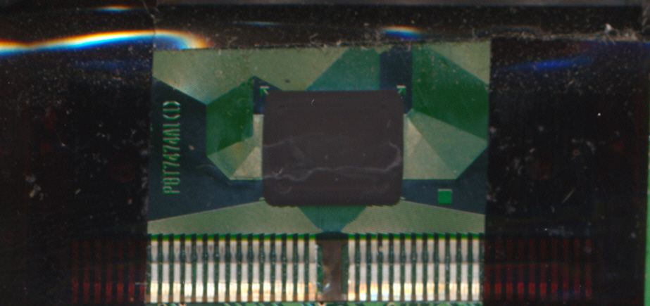
Datamath attributes the LCD module photographed from a March 2004 TI-84 Plus
to Toshiba T6K04. The photograph shows the controller area under opaque
epoxy, so it does not expose a readable die marking. The identification is a
source-attributed module record rather than a marking read from the image.
[standard]
The local ROM uses only visible columns 0–11 in its full-screen clear and
graph blit loops. It does not distinguish the 15-byte T6A04A row from the
16-byte T6K04 row. Datamath’s attribution supplies revision-specific external
evidence that the ROM cannot. [confirmed] for the ROM access range; [standard]
for the March 2004 controller attribution.
Coordinate vocabulary
Toshiba documentation names the pixel row X and the byte column Y. Software often uses the opposite convention. This page uses row for 0–63 vertically and byte column for the horizontal group selected by commands 0x20–0x3F.
| Quantity | Command or transfer | Visible range |
|---|---|---|
| Row | command 0x80 + row | 0x80–0xBF |
| Byte column | command 0x20 + column | 0x20–0x2B |
| Pixel within a byte | data bit 7 through bit 0 | left to right [standard] |
| Visible storage | 12 byte columns × 64 rows | 768 bytes |
The Z-address command 0x40 + shift changes which controller row appears at the top of the panel. It does not copy video RAM. Rows wrap modulo 64 when displayed. [standard]
Ordinary 8-bit addressing. The TilEm skin locates the controller model on the calculator face. The visible 12-byte row and OS command ranges are [confirmed]; the T6K04’s 16-byte controller row, read latch, and off-screen storage are [standard].
Port interface
| Port | Direction | Role |
|---|---|---|
0x10 | read | controller status |
0x10 | write | controller command |
0x11 | read/write | latched video-RAM data at the current address |
0x12 | read/write | second-chip-select mirror of 0x10 on documented ASIC revisions [standard] |
0x13 | read/write | second-chip-select mirror of 0x11 on documented ASIC revisions [standard] |
0x02 bit 1 | read | ASIC LCD-wait timer ready at high CPU speed |
0x2F | read/write | duration selector for the ASIC LCD-wait timer |
The OS paths decoded here use 0x10 and 0x11. The resolved calculator trace contains no port-0x12 or port-0x13 LCD transaction. [confirmed] for the trace; [standard] for the physical mirrors.
Controller-side signals
The T6K04 exposes an 8-bit DB0–DB7 bus for an 80-series processor. Its
D/I input distinguishes command bytes from display-data bytes, /WR selects
reading or writing, and /CE strobes the transfer. /RST resets the
controller. /STB stops its oscillator, rejects commands and data, and drives
the LCD supply outputs to VDD. The calculator ASIC turns port instructions
into these controller-side operations, so Z80 code does not toggle the
individual signals. [standard]
The T6K04 includes 128 column outputs, 64 row outputs, display RAM, an oscillator, contrast control, five LCD-supply operational amplifiers, and a DC–DC converter with doubler, tripler, and quadrupler modes. Its logic supply range is 2.7–5.5 V, and Toshiba specifies a tape-carrier package (TCP). Replacement controllers can expose compatible port behavior without reproducing every internal analog block or off-screen RAM cell. [standard]
Status read
Reading port 0x10 returns the controller state: [standard]
| Bit | Meaning |
|---|---|
| 0 | increment direction when set; decrement when clear |
| 1 | movement affects the byte column when set; row when clear |
| 2 | fixed zero in the T6K04 status definition |
| 3 | LCD-supply operational amplifier enabled when set |
| 4 | controller reset state |
| 5 | display enabled |
| 6 | 8-bit transfer mode when set; 6-bit mode when clear |
| 7 | controller busy on controllers that implement a reliable busy flag |
Late replacement controllers can move the internal video-RAM pointer when software reads status. Busy-poll loops that work on Toshiba controllers can therefore corrupt addressing on those units. WikiTI recommends a fixed delay or the ASIC delay mechanism for cross-revision code. [standard]
OS 2.55MP avoids this incompatibility in its common path: lcd_wait at ram:0CC3 reads port 0x02, not port 0x10. [confirmed]
Command set
The table separates public controller behavior from the subset used by this ROM.
| Command | Meaning | OS 2.55MP use |
|---|---|---|
0x00 | select 6-bit transfers | used by some text read/modify/write paths at 01:5AD3 [confirmed] |
0x01 | select 8-bit transfers | _LCD_DRIVERON and _PutMap [confirmed] |
0x02 | disable display output while retaining video RAM | lcd_disable at ram:0CD9; _PowerOff calls it [confirmed] |
0x03 | enable display output | _LCD_DRIVERON [confirmed] |
0x04 | decrement row after each data transfer | documented controller mode [standard] |
0x05 | increment row after each data transfer | OS vertical byte loops [confirmed] |
0x06 | decrement byte column after each data transfer | documented controller mode [standard] |
0x07 | increment byte column after each data transfer | OS horizontal row blits [confirmed] |
0x08–0x0B | select the duration of enhanced LCD-supply amplifier drive | _LCD_DRIVERON selects 0x08 or 0x0B [confirmed]; T6K04 OPA2 behavior [standard] |
0x0C–0x0F | mirroring controls reported on newer controllers | absent from the T6K04 command table and unused by this ROM [standard] |
0x10–0x17 | control LCD-supply amplifier state and ability; 0x14–0x17 keep it on | _LCD_DRIVERON selects 0x16 or 0x17 [confirmed]; T6K04 OPA1 behavior [standard] |
0x18–0x1F | T6K04 test-mode select | Toshiba says not to use this range; WikiTI separately reports 0x18 as test-mode exit and warns that high-drive modes can damage the panel [standard] |
0x20–0x2F | set T6K04 byte column in 8-bit mode | visible OS range 0x20–0x2B [confirmed]; 16-column limit [standard] |
0x20–0x35 | set T6K04 six-pixel group in 6-bit mode | OS selects 6-bit mode in an edge-rendering path [confirmed]; 22-entry limit [standard] |
0x40–0x7F | set displayed top-row offset | _LCD_DRIVERON writes 0x40 [confirmed] |
0x80–0xBF | set row | full 64-row range [confirmed] |
0xC0–0xFF | set controller contrast 0–63 | _LCD_DRIVERON derives the command from contrast [confirmed] |
The T6K04 defines contrast command 0xC0 as brightest and 0xFF as darkest.
The power and test commands affect analog drive circuitry and vary across
controller revisions. TilEm ignores them except for display enable, display
disable, and contrast. [standard]
Reset and standby states
Driving T6K04 /RST low selects 8-bit transfers, byte-column increment, row
and byte-column address zero, displayed top-row offset zero, display off,
LCD-supply amplifier on at minimum ability, minimum enhancement, and minimum
contrast. The status reset bit remains set while the controller is held in
reset. Toshiba’s reset-state list does not state that display RAM is cleared.
[standard]
Driving /STB low stops the oscillator, prevents command and data acceptance,
reduces controller power, and drives VLC1–VLC5 to VDD. The OS’s display
disable command 0x02 is a separate operation and does not clear display RAM.
[standard]
Data transfers and address movement
Port 0x11 transfers one unit at the current row and byte column, then applies command 0x04, 0x05, 0x06, or 0x07. [standard]
In 8-bit mode, all eight data bits map to adjacent pixels. In 6-bit mode, only bits 0–5 are significant and the controller packs six-pixel groups. The OS initializes 8-bit mode for ordinary full-screen work but temporarily selects 6-bit mode in large-font edge handling at 01:5AD3. [confirmed]
Read latch and dummy reads
Controller reads are one transfer behind the addressed video-RAM byte. After a row or column command, the first port-0x11 read returns the old output latch; the read loads the newly addressed byte into that latch. Software must discard one dummy read and use the second. Auto-increment or auto-decrement does not require another dummy read between sequential bytes. [standard]
lcd_read_data at 01:5A60 performs exactly two reads: [confirmed]
01:5A60  call ram:0CC3
01:5A63  in a,(0x11)       ; discard stale output latch
01:5A65  call ram:0CC3
01:5A68  in a,(0x11)       ; addressed byte
The routine then restores an OS-tracked row command from 0x8451 and selects row-increment mode. lcd_write_data at 01:5A59 is the matching wait plus OUT (0x11),A. These routines transfer arbitrary pixel data; neither routine sets or reads contrast. [confirmed]
Bounds and wrap behavior
The T6K04 data sheet defines byte-column commands 0x20–0x2F in 8-bit mode
and six-pixel group commands 0x20–0x35 in 6-bit mode. Its address counter
wraps across 16 or 22 entries respectively. Toshiba says not to issue a byte
column beyond 15 in 8-bit mode. [standard]
WikiTI reports that some Toshiba command decoders accept the wider
0x20–0x3F field, while transfers outside implemented RAM do not change RAM.
That out-of-range behavior is outside the T6K04 data-sheet contract and varies
across controllers and emulators. [standard]
The row coordinate wraps across 64 rows. The controller-specific byte-column width is one reason software should not use off-screen RAM as portable storage. [standard]
ASIC-side wait timing
At high CPU speed, each access to ports 0x10–0x13 clears port-0x02 bit 1 for a programmable interval. Port 0x2F selects that interval in nominal 64-T-state steps with values 48, 112, 176, 240, 304, 368, 432, or 496 T-states. CPU-speed value 1 uses bits 0–1; value 2 uses bits 2–4; value 3 uses bits 5–7. CPU-speed value 0 leaves port-0x02 bit 1 set. [standard]
Ports 0x29–0x2C separately add T-states to the LCD-port instruction and
gate the Flash/RAM waits in port 0x2E. Bus timing and wait states
reconstructs the complete joint register block and both emulator models.
The retail boot page writes 0x4B to port 0x2F at 3F:41D3. With the OS’s normal CPU-speed value 1, the low field is 3, selecting 240 T-states. At nominal 15 MHz this interval is 16 µs. [confirmed] for the writes and trace; [standard] for the hardware timer interpretation.
The T6K04 data sheet specifies its internal busy interval as $2/f_{OSC} \leq T \leq 4/f_{OSC}$. For a 35 Hz common drive, its four frequency-select examples use 28.56, 57.12, 228.48, and 456.96 kHz. They imply the following controller-busy ranges: [standard]
| Example $f_{OSC}$ | T6K04 busy range |
|---|---|
| 28.56 kHz | 70.03–140.06 µs |
| 57.12 kHz | 35.01–70.03 µs |
| 228.48 kHz | 8.75–17.51 µs |
| 456.96 kHz | 4.38–8.75 µs |
Toshiba rates the oscillator input from 20 to 500 kHz and warns that mounting conditions affect an external-resistor oscillator. The module photograph does not resolve the frequency-select wiring or resistor value. The OS’s 16 µs ASIC wait therefore cannot identify the fitted oscillator or prove worst-case controller margin by itself. [standard] for the T6K04 limits; [hypothesis] for the board-specific oscillator and margin.
The controller’s /CE switching limits are a separate timing layer. Toshiba
specifies the following values at 25 °C: [standard]
| Logic test condition | Minimum /CE cycle | Minimum /CE pulse | Minimum address setup | Minimum write-data setup | Maximum read-data delay |
|---|---|---|---|---|---|
| 3.0 V ± 10% | 1,000 ns | 450 ns | 100 ns | 280 ns | 350 ns |
| 5.0 V ± 10% | 500 ns | 220 ns | 60 ns | 60 ns | 160 ns |
These limits constrain the ASIC-to-controller strobe. The port-0x2F interval
instead prevents the next access while the controller’s internal operation can
remain busy. Z80 instruction timing does not reveal the /CE waveform, so the
physical strobe still requires a bus capture. [standard] for the controller
limits; [hypothesis] for the ASIC waveform.
lcd_wait preserves AF and spins on that ASIC-ready bit: [confirmed]
ram:0CC3  push af
ram:0CC4  in a,(0x02)
ram:0CC6  and 0x02
ram:0CC8  jr z,ram:0CC4
ram:0CCA  bit 3,(iy+0x41)
ram:0CCE  call nz,ram:0CE6
ram:0CD1  call nz,ram:0CE6
ram:0CD4  call nz,ram:0CE6
ram:0CD7  pop af
ram:0CD8  ret
The three optional calls add fixed instruction delay when the OS flag at IY+0x41 bit 3 is set. That byte is shared with USB state in the published equates; the local code establishes the delay effect but does not establish an LCD-specific public name for the flag. [confirmed]
lcd_write_command_a at ram:0CDB repeats the port-0x02 wait and writes A to port 0x10. lcd_disable at ram:0CD9 loads command 0x02 and enters that helper. [confirmed]
Controller initialization
_LCD_DRIVERON = 4978 has body 06:4D02. It sends every command through lcd_write_command at 06:4D35, which calls lcd_wait before writing port 0x10. [confirmed]
| Order | Command | Effect |
|---|---|---|
| 1 | 0x40 | top displayed row = controller row 0 |
| 2 | 0x05 | increment row after data transfers |
| 3 | 0x01 | select 8-bit transfer mode |
| 4 | 0x03 | enable display output |
| 5 | 0x16 or 0x17 | select one of the upper LCD-supply amplifier abilities |
| 6 | 0x08 or 0x0B | select amplifier-enhancement duration |
| 7 | 0xC0 OR (contrast + 0x18) | program contrast |
Calls to the hardware test at ram:1837 choose between the two power values. In the resolved TI-84 Plus TilEm trace, the sequence is:
40 05 01 03 17 0B EF
The final 0xEF means controller contrast 0x2F. The RAM byte contrast at
0x8447 was 0x17, and _LCD_DRIVERON added 0x18. Toshiba defines larger
T6K04 contrast arguments as darker, from brightest 0xC0 to darkest 0xFF.
[confirmed] for the ROM arithmetic; [standard] for the controller direction.
The trace records this sequence twice during cold startup before the homescreen clear. This is OS behavior under the traced startup path, not a requirement that user code initialize the controller twice. [confirmed]
Full-screen clear
_ClrLCDFull = 4540 has body 01:60E4. It temporarily clears the run-indicator flag, then invokes _ClearRow at 01:6934 for row bases 0xB8, 0xB0, …, 0x80. Each call clears an eight-row band. [confirmed]
For each byte column 0x20–0x2B, _ClearRow performs: [confirmed]
- send command
0x07throughlcd_mode_column_increment; - restore the band-base row command;
- send command
0x05throughlcd_mode_row_increment; - select the current byte column;
- write eight zero bytes while the row auto-increments;
- advance to the next byte column.
The arithmetic covers every visible byte exactly once:
$$ 8\text{ bands} \times 12\text{ columns} \times 8\text{ rows} = 768\text{ writes} $$
The resolved trace shows the first band as row command 0xB8, column commands 0x20 through 0x2B, and eight zero data writes after every column command. The next band begins at 0xB0; the final band begins at 0x80. [confirmed]
Dormant boot-page display test
Retail page 3F contains boot_lcd_keypad_diagnostic at 3F:4658. Its only
incoming branch, boot_diagnostic_gate at 3F:4615, follows XOR A,
OUT (0x05),A, and CP 0x09, so it is constant-false. The dormant MODE diagnostic branch
can execute boot_ram_test at 3F:461A, but it cannot continue into this LCD
routine under Z80 semantics. [confirmed]
The dormant code fills all 768 visible bytes through boot_lcd_fill_pattern at
3F:46EF and overwrites individual full rows through boot_lcd_write_row at
3F:472E. It presents six patterns. The sequence includes solid 0xFF and
0x00, alternating 0x55/0xAA and 0x00/0xFF rows, a solid 0xAA
pattern, and a bordered 0x81 pattern. It then sweeps raw contrast commands
0xFF through 0xD9 and
restores the OS contrast byte through boot_lcd_restore_contrast at
3F:74F5. [confirmed]
An explicit direct-entry Wabbitemu harness validates the actual retail helpers,
including 768 data writes from boot_lcd_fill_pattern (3F:46EF), 12 data
writes from boot_lcd_write_row (3F:472E), and the 0xFF output from
boot_lcd_write_contrast (3F:74F8).
This is emulator agreement with executed ROM,
not evidence that retail boot reaches the code or that a physical panel
produces the modeled image. [confirmed] for pinned Wabbitemu commit 48c2dc0;
[hypothesis] for unmeasured physical output. See
Retail boot hardware initialization
for the stage and keypad flow.
Graph-buffer transfer
plotSScreen at 0x9340 is the 768-byte row-major graph buffer. _GrBufClr at 04:6071 clears it with one zero store followed by LDIR of 0x02FF bytes; it does not access the LCD. [confirmed]
_GrBufCpy at 04:60A3 enters the controller-transfer core at 04:6176. The TI-84 Plus direct-RAM path performs these operations for each selected pixel row: [confirmed]
- command
0x07selects byte-column auto-increment; - a command in
0x80–0xBFselects the row; - command
0x20selects visible byte column 0; - 12 sequential data writes copy one row from the RAM buffer;
- the source pointer and row command advance.
The caller adjusts the starting row and row count for full-screen and split-screen states. The controller loop therefore treats the transfer extent as state, while the row width remains 12 bytes. [confirmed]
The alternative path calls lcd_write_block at ram:18B1 when the source lives in banked RAM. That helper temporarily maps RAM page 0x83 through port 0x06, writes B bytes to port 0x11, restores the prior mapping, and restores the caller’s interrupt-enable state. [confirmed]
Text drawing and read-modify-write
Homescreen text does not render through plotSScreen. _PutMap at 01:5A98 loads an eight-byte large-font record and writes the controller directly. It selects row and byte-column commands from curRow and curCol, then emits the glyph through port 0x11. [confirmed]
When a glyph overlaps an existing byte boundary, _PutMap reads controller RAM, combines glyph bits with the retained pixels, and writes the result back. The read helpers at 01:5A70 and 01:5A7A perform the required dummy plus real reads before restoring the row and movement mode. [confirmed]
This creates two independent software representations:
| State | Address | Role |
|---|---|---|
| Controller video RAM | external LCD controller | currently scanned panel image |
plotSScreen | 0x9340–0x963F | graph/back buffer; copied explicitly |
saveSScreen | 0x86EC–0x89EB | saved 768-byte display image |
textShadow | 0x8508–0x8587 | 16×8 homescreen character shadow |
lFont_record | 0x845A–0x8461 | current eight-byte large-font render record |
Changing one RAM buffer does not update the panel until a routine copies or renders it. Direct text writes can likewise change controller RAM without changing plotSScreen. [confirmed]
Screen reads and saved displays
lcd_read_block at ram:1890 reads B bytes from port 0x11 into banked RAM. It temporarily maps RAM page 0x83, preserves the previous port-0x06 value, and restores the caller’s interrupt state. The caller must establish the controller address and consume any required dummy read before a sequential block. [confirmed]
_SaveDisp at 39:5DD8 accepts the destination in HL. At 39:5DFF, it tests
bit 7 of H: a destination below 0x8000 uses the page-83 helper through
CALL ram:1890 at 39:5E03; a destination at or above 0x8000 uses the direct
RAM loop at 39:5E08. The saved-page caller’s dynamic trace records the
768-byte capture extent, but the bcall is not restricted to that destination.
_RestoreDisp later copies saved image data through the display paths. [confirmed]
Contrast and power-off
The OS stores its user-facing contrast level at 0x8447. _LCD_DRIVERON adds 0x18, forces command bits 0xC0, and sends the result. Code that writes a raw controller contrast command without updating 0x8447 can cause the next OS contrast adjustment or driver initialization to jump to a different level. [confirmed] for OS state; [standard] for direct-hardware callers.
Display-disable command 0x02 blanks the panel but leaves controller video RAM available. The ASIC’s low-power transition is separate. _PowerOff calls lcd_disable at ram:0CD9, performs OS cleanup, then uses port 0x03 plus HALT to enter low power. See Clock, timers, and power. [confirmed]
Dynamic I/O trace
The trace resolver can print decoded I/O instructions after resolving every banked program counter:
nix develop -c python3 -m ti84re.trace.resolve \
  /tmp/tilem-validation-home2plus3.trace \
  --initial-mapping ti84p-reset --names tools/symbols/names.txt \
  --io-ports 10-13,2f --io-count 360
The trace captures three load-bearing sequences: [confirmed]
- boot writes
0x4Bto port0x2Fat3F:41D3; _LCD_DRIVERONwrites40 05 01 03 17 0B EFat06:4D38;_ClrLCDFullwrites the eight-band, 12-column, eight-byte clear pattern through01:5A95,01:6945, and01:694B.
The trace is an emulator execution record. It proves the ROM path and values but does not prove analog power behavior, physical busy duration, or controller-revision quirks.
Emulator comparison
All four emulators implement the commands and visible 12-byte rows used by OS 2.55MP. Their hidden-column, busy, and ASIC-timer behavior differs. These differences are emulator test cases, not physical-controller evidence. [standard]
| Area | TilEm f56ad63 | Wabbitemu 48c2dc0 | MAME 0.287 | jsTIfied 20170706a |
|---|---|---|---|---|
| Controller RAM | 1,024 bytes, 16 × 64 | 1,024 bytes, 16 × 64 | 960 bytes, 15 × 64 | 960 bytes, 15 × 64 |
| 8-bit column increment | accesses 0–15, then normalizes to 0 | accesses 0–14, then wraps to 0 | counts modulo 32 without a RAM bound | accesses 0–14 around a 120-pixel row |
| Controller busy | 50 or 70 cycles; early transfers rejected | 60-T-state guard from the last accepted write | absent; busy status is always zero | randomized 25–47-emulator-cycle interval |
| ASIC ready | port-0x2F timer starts on every LCD read or write | interval measured from the last accepted write | port-0x02 bit 1 is always set | status derives from the emulator’s LCD timer |
Ports 0x12/0x13 | aliases | absent | aliases | aliases |
| Data-read latch | modeled | modeled | modeled | modeled |
| Analog power and test modes | ignored | ignored | values partly stored; no analog effect | drive fields and grayscale display physics modeled |
| Driver status | active TI-84 Plus trace target | source model | MACHINE_NOT_WORKING | browser emulator source model |
TilEm behavior and fidelity gaps
TilEm models the controller and the ASIC wait timer as separate mechanisms. [standard]
| Area | TilEm behavior | Fidelity consequence |
|---|---|---|
| Video RAM | fixed 1,024-byte array, 16 bytes × 64 rows | capacity matches T6K04, but not 120-pixel or no-extra-RAM variants |
Ports 0x12/0x13 | aliases command/status and data | models the documented second-chip-select mirrors |
| Controller busy | 50 emulated cycles after an accepted access | direct too-fast accesses are ignored when delay emulation is enabled |
| ASIC wait | port-0x02 bit 1 remains clear for the port-0x2F interval | reproduces the OS wait loop independently of controller busy |
| I/O overhead | adds the configured LCD_PORT_DELAY per LCD-port access; defaults are 5/9/11/14 cycles by speed mode | emulator policy, not a physical bus measurement |
| Read latch | returns nextbyte, then loads the addressed byte | reproduces the dummy-read requirement |
| 6-bit mode | packs six-pixel writes into the internal byte array | supports OS edge-rendering paths |
| Z address | displays (row + shift) mod 64 | reproduces vertical display rotation |
| Power/test/mirror commands | mostly ignored | does not model analog drive, blue test modes, or newer-controller mirroring |
| Status-read pointer quirk | not modeled | cannot reproduce late Novatek corruption from busy polling |
| Out-of-range columns | wraps against the fixed 16-byte stride before transfer | differs from documented behavior on narrower controllers |
| Low power | frame output blanks when the LCD is inactive or the halted ASIC powers down | approximates visible power state rather than electrical retention |
TilEm reset initializes controller contrast to 32, 8-bit mode, byte-column increment, row and column zero, and display disabled. It does not clear the LCD backing array. A guarded direct-core reset retains a seeded display byte while rebuilding every controller field above. OS initialization then replaces the controller values. [standard] for source; [confirmed] for the pinned run.
Wabbitemu behavior and fidelity gaps
Wabbitemu allocates 16 bytes for each of 64 controller rows and displays the first 96 pixels. It decodes the same command groups as TilEm. Power and test commands have no controller effect. Its rendering queue uses repeated frames to approximate grayscale, which is a frontend policy rather than monochrome controller behavior. [standard]
The 8-bit column-increment path wraps when the next column reaches 15. It
therefore visits columns 0–14; TilEm visits 0–15. A direct command can
still select column 15. Wabbitemu indexes that direct coordinate modulo its
16-byte row. Commands 0x30–0x3F therefore alias columns 0–15 instead of
following the documented out-of-range behavior. [standard]
Wabbitemu rejects command and data transfers made within 60 T-states of the
last accepted LCD write. An early status read returns 0x80; an early data
read or write is discarded. Accepted data reads advance the pointer and output
latch but do not update the guard’s timestamp. [standard]
Its separate port-0x02 ready calculation also measures from the last accepted
write. It applies the port-0x2F field as $48 + 64n$ T-states. The speed-selected
ports 0x29–0x2C add their shifted instruction delay before either LCD port
handler. This agrees with the register arithmetic, but the triggering event
differs from TilEm’s every-access timer. [standard]
Wabbitemu registers ports 0x10 and 0x11 for this model but not the documented
0x12 and 0x13 aliases. It subtracts a model-specific base level of 24 from
contrast commands before its grayscale renderer consumes the value. This
display calibration is not controller voltage evidence. [standard]
A guarded initialized-core run at 48c2dc0 confirms these Wabbitemu-specific
edges dynamically: [standard]
| Case | Native observation |
|---|---|
| Controller guard | a status read at 59 T-states returns busy 0x80; one at 60 T-states is accepted |
| Early write | a data write at 59 T-states leaves the cell and pointer unchanged |
| Increment from column 14 | writes visit columns 14, 0, 1, and 2; column 15 remains unchanged |
| Direct hidden columns | command column 15 accesses column 15; command column 31 aliases the same cell and wraps the pointer to 0 |
| Read latch | three accepted reads return 0x00, 0x12, and 0x34 from cells containing 0x12, 0x34, and the following byte |
| Read timestamp | three same-T-state reads advance the pointer without changing the last-successful-write timestamp |
| Port map | reads of absent ports 0x12 and 0x13 are rejected and produce adapter fallback 0xFF |
Wabbitemu’s low-level CPU_reset leaves the complete LCD object unchanged.
The frontend calc_reset then invokes the LCD reset callback. A guarded
frontend-equivalent call disables output; zeros x, y, z, the last-read
latch, display RAM, and the grayscale queue; selects 8-bit words; and sets
contrast 32. It retains the last-access T-state and lcd_delay field. This is
frontend policy, not physical controller retention. [standard] for source;
[confirmed] for the pinned initialized-core run.
The LCD reset callback stores word_len = 8, while its status expression
shifts the field as though it were Boolean. The reset-state controller transfers
eight-bit data, but the first accepted status after display enable is 0x23,
with bit 6 clear. Sending command 0x01 stores Boolean one, after which the
same status is 0x63. This is a Wabbitemu state-representation defect, not
evidence for a physical reset status. [standard]
MAME behavior and fidelity gaps
MAME 0.287 attaches a generic T6A04 device to ports 0x10–0x13. Its 960-byte
array matches a 15-byte by 64-row controller. The OS-visible 12 columns, address
movement, Z shift, display enable, 6-bit packing, and dummy-read latch are
implemented. [standard]
The five-bit column pointer is not checked against the 15-byte stride before a
data read or write. Column 15 on row 0 indexes byte 15, which is row 1 column 0
in the backing array. Column 31 on row 63 computes index 976, beyond the
960-byte array. The OS stays within columns 0–11, so its ordinary clear and
blit loops do not trigger this C++ out-of-bounds path. [standard]
The device source lists busy and contrast among its TODO items. The busy flag never becomes one. Contrast commands update a field, but screen rendering does not consume it. MAME stores the two power-control fields without modeling their analog effect. [standard]
The TI-84 Plus driver returns port-0x02 with bit 1 permanently set and does
not map ports 0x29–0x2F. The ROM’s lcd_wait loop therefore exits on its
first read, and no speed-selected LCD instruction delay is applied. The driver
is marked MACHINE_NOT_WORKING; these omissions do not describe the ASIC.
[standard]
Native MAME confirmation. The guarded CPU-I/O-space probe reads the untouched controller startup state before seeding later independent cases. Ports 0x10 and 0x12 both return status 0x43. All 960 backing bytes are zero, and the row, column, Z address, output latch, and display-enable fields are zero. Eight-bit mode, column movement, and increment direction are selected. Port 0x02 returns 0xC3. [standard]
Four immediate status reads after display enable all return 0x63; busy bit 7 remains clear. Movement commands 0x04–0x07 produce statuses 0x60, 0x61, 0x62, and 0x63. Word-length commands change the status between 0x23 and 0x63. A display-off write through port 0x12 is visible at port 0x10, and a display-on write through port 0x10 is visible at port 0x12. Contrast 0xEF, OPA1 0x17, OPA2 0x0B, and Z-address 0x7F store 0x2F, 3, 3, and 0x3F. [standard]
Four incrementing writes from row 0, column 14 store A0 A1 A2 A3 at array indices 14–17 and leave column 0x12. A direct row-0 column-15 write reaches index 15, which is row 1 column 0 in the 15-byte stride. Row-0 column 31 reaches index 31, which is row 2 column 1, then wraps the pointer to zero. Sequential reads over bytes 0x12, 0x34, and 0x56 return 0x00, 0x12, and 0x34. Two 6-bit writes of 0x3F and 0x15 pack into bytes 0xFD and 0x50. [standard]
Ports 0x29–0x2F return seven zero bytes before and after patterned writes. Two isolated runs produce byte-identical native reports with SHA-256 d6930650a96383710be7ebb772675b5a494cba2450827b12a535c963fa464bfc. The probe does not execute row 63, column 31; the source-computed index 976 remains an unexecuted unsafe case. [standard]
Reproducing pointer differences
tools/ti84re/hardware/lcd_controller.py provides the source-attributed T6K04 specification,
vendor busy-time calculation, command decoding, status composition, the
dummy-read latch, and source-modeled pointer walks. The hardware report keeps
the module attribution and its photographic limit together:
$ python3 -m ti84re.hardware.describe_lcd_controller hardware
reported controller: Toshiba T6K04
  calculator evidence: Datamath caption for a March 2004 TI-84 Plus module
  limit: controller die is hidden under epoxy; no marking is visible
  data sheet: 128x64 pixels, 8192 bits, 16 8-bit pages
  interface: 8-bit 80-series MPU; logic supply=2.7-5.5 V; package=TCP
  3 V bus: cycle>=1000 ns pulse>=450 ns read-delay<=350 ns
  5 V bus: cycle>=500 ns pulse>=220 ns read-delay<=160 ns
The exact data-sheet formula can be evaluated at Toshiba’s four example oscillator choices:
$ python3 -m ti84re.hardware.describe_lcd_controller busy
fOSC=28.56 kHz: 70.028-140.056 us
fOSC=57.12 kHz: 35.014-70.028 us
fOSC=228.48 kHz: 8.754-17.507 us
fOSC=456.96 kHz: 4.377-8.754 us
The pointer CLI compares an increment starting at hidden column 14:
$ python3 -m ti84re.hardware.describe_lcd_controller walk --row 0 --column 14 --movement 7 --count 3
TilEm
  0: requested=(0,14) access=(0,14) index=14 next=(0,15)
  1: requested=(0,15) access=(0,15) index=15 next=(0,16)
  2: requested=(0,16) access=(0,0) index=0 next=(0,1)
Wabbitemu
  0: requested=(0,14) access=(0,14) index=14 next=(0,0)
  1: requested=(0,0) access=(0,0) index=0 next=(0,1)
  2: requested=(0,1) access=(0,1) index=1 next=(0,2)
MAME
  0: requested=(0,14) access=(0,14) index=14 next=(0,15)
  1: requested=(0,15) access=(0,15) index=15 next=(0,16) [column-out-of-range]
  2: requested=(0,16) access=(0,16) index=16 next=(0,17) [column-out-of-range]
The hardware, busy, decode, profiles, status, and latch subcommands
accept --json for scripts. Transfer reports distinguish a controller column
outside the modeled row from an index outside the complete backing array.
tools/ti84re/emulators/wabbitemu/run_lcd_edge_probe.py runs the guarded dynamic matrix. It
requires the exact OS 2.55MP ROM, records the ROM and native-binary hashes, and
checks every field through tools/ti84re/emulators/wabbitemu/lcd_probe.py. The ROM is only an
initialized-core fixture in this mode; no TI-OS instruction executes.
tools/ti84re/emulators/wabbitemu/run_lcd_diagnostic_probe.py is a separate direct-entry mode.
It boots the exact ROM to its protection baseline, then executes
boot_lcd_initialize, boot_lcd_fill_pattern, boot_lcd_write_row, and
boot_lcd_write_contrast from an injected RAM harness.
Its manifest labels the run as direct entry and retains compact counters and
screen hashes rather than an instruction log.
tools/ti84re/emulators/mame/lcd.py parses the MAME state, pointer, latch, packing, and port-map
matrix against tools/ti84re/hardware/lcd_controller.py. The guarded CLI retains the exact
MAME, ROM, Lua-adapter, output, and evidence-scope identities:
mame_lcd_parent=$(mktemp -d /tmp/ti84-mame-lcd.XXXXXX)
nix shell nixpkgs#mame --command python3 -m ti84re.emulators.mame.run_lcd_probe \
  --expected-mame-sha256 \
    fc5f4aba1aa6eb115d66decad13bb3f5313b9f3be9cff7c785d8d88e3fca0b91 \
  --output-dir "$mame_lcd_parent/run" --json
Resolved findings and open hardware questions
- [confirmed] OS 2.55MP waits through port-
0x02bit 1 and does not busy-poll port0x10inlcd_wait. - [confirmed]
01:5A59and01:5A60write and read pixel data; they are not contrast helpers. - [confirmed]
_LCD_DRIVERONemits0x40,0x05,0x01,0x03, hardware-dependent power commands, and a RAM-derived contrast command. - [confirmed]
_ClrLCDFullcovers all 768 visible bytes with eight vertical bands. - [confirmed]
boot_lcd_keypad_diagnosticcovers all 12 visible columns, butboot_diagnostic_gateis constant-false. - [confirmed]
_GrBufClrchanges only RAM, while_GrBufCpyperforms the controller transfer. - [confirmed]
_PowerOffdisables display output before the ASIC enters low power. - [standard] Datamath attributes the photographed March 2004 module to Toshiba
T6K04, whose primary data sheet specifies 128×64 RAM. The die is hidden under epoxy, so the photograph does not independently expose its marking. - [hypothesis] The exact controller and off-screen RAM behavior still require per-calculator identification or measurement outside that source-attributed March 2004 module.
- [hypothesis] The late-controller status-read pointer mutation, power-command analog effects, and off-screen retention need physical tests across TA2/TA3 board revisions.
- [hypothesis] TilEm’s configured LCD I/O delay and controller busy period should be compared with bus captures rather than treated as hardware constants.
- [standard] Wabbitemu’s 15-column increment cycle and write-based ready timer, plus MAME’s unchecked 15-byte row, are emulator limits rather than hardware results.
- [standard] A guarded MAME run verifies its startup state, status and command decode, permanent busy-clear state, mirror ports, safe hidden-column aliases, dummy-read latch, 6-bit packing, stored analog fields, constant ASIC-ready bit, and missing delay ports.
- [hypothesis] Physical tests should sweep hidden columns and time readiness after reads and writes independently.
Sources
| Source | Used for |
|---|---|
WikiTI port 0x02 | ASIC LCD-ready bit and high-speed behavior |
WikiTI port 0x10 | status bits, commands, addressing, controller variants, busy-poll incompatibility, and power/test cautions |
WikiTI port 0x11 | pixel data, output latch, dummy reads, 6-bit transfers, and transfer delay |
WikiTI ports 0x12 and 0x13 | second-chip-select mirrors |
WikiTI port 0x2F | ASIC wait-duration fields and defaults |
| Datamath March 2004 TI-84 Plus module and LCD photograph | source-attributed T6K04 identity and the epoxy-covered module construction |
| Toshiba T6K04 data sheet, 2001-03-13 | exact 128×64 RAM, command and status tables, counter bounds, dummy reads, reset state, bus timing, oscillator choices, busy formula, supply range, and package; PDF SHA-256 e53bcf3f12c1cba2011b886ab196b6e1827aea4c1a2d9fb28c3d6d501d986577 |
| Toshiba T6A04A data sheet | compatible earlier 120×64 controller and family comparison |
TilEm lcd.c, calcs.c, x4_io.c, and x4_init.c | emulator video RAM, command decode, latches, port aliases, wait timers, and reset state |
Wabbitemu lcd.c, 83psehw.c, and calc.c | controller RAM, pointer movement, transfer guard, ASIC-ready calculation, port registration, and frontend reset scope |
MAME t6a04.cpp, ti85.cpp, and ti85_m.cpp | controller array and commands, TI-84 Plus port map, fixed ready bit, and driver status |
jsTIfied deployed 20170706a artifact and readable mirror | fourth controller model, 120-pixel storage, randomized busy interval, latch, and display physics |